SU-8 Testing ( v1g)
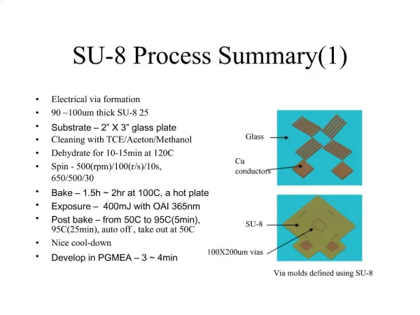
SU-8 Testing ( v1g). Thin SU8 on glass slide Test: Soft Bake (SB) and Post Exposure Bake (PEB). “ Control ” Recipe. Spin Coating: 10 s @ 500 rpm ; 30 s @ 2000 rpm expected thickness: 600 nm Soft Bake (SB): 60 s @ 93°C Exposure: 8 s @ 275 W PEB: 60s @ 93°C

SU-8 Testing ( v1g)
E N D
Presentation Transcript
SU-8 Testing (v1g) Thin SU8 on glass slide Test: Soft Bake (SB) and Post Exposure Bake (PEB)
“Control” Recipe • Spin Coating: 10 s @ 500 rpm; 30 s @ 2000 rpm • expected thickness: 600 nm • Soft Bake (SB): 60 s @ 93°C • Exposure: 8 s @ 275 W • PEB: 60s @ 93°C • Develop: 4 min in SU8 developer • SU8 developer rinse • IPA rinse/Nitrogen Dry
1st Set of Tests • 4 samples; 8 devices/sample • 4 Wells (W)+4 Blanks (B)/sample • S1: “Control”: Misaligned (see next slide); All shorted; R(W) ~ 8.6 Ω; R(B) ~ 10 Ω Test Parameters for S2-4: • SB (RT Evap) and PEB @ 60°C, same times for each • S2: 8 min: R(W) = (2.7±0.8) Ω; R(B) = (11±0) MΩ; C(B) = (15.0 ± 0.1) pF • S3: 13 min: Also misaligned (see next slide) R(W) = (4.9±?) Ω; R(B) = (6 ± 8) MΩ; C(B) = (17.0 ± 0.5) pF • S4: 15 min: R(W) = (4 ± 1) Ω; R(B) = (11±0) MΩ; C(B) = (17 ± 0) pF • Cracking patterns seen in S2, S3, S4
Findings/Discussion 1st Set • “Control”: All shorted • The “misalignment” ONLY causes • Top contacts don’t fully overlap guide circles on bottom that could result in the top contact not covering the well(is this the case? If not say so) – will NOT cause short • Top contacts touching two exposure regions • either single + double exposures (normal) – NOT cause short, • or single + no exposures (should not happen but may - according to Mark, but microscopy can tell us – presence of a well – check to confirm and revise here …) – MAY cause short (ONLY no exposure) • RT Evap+ PEB @ 60°C at various times: All good • All Wells are shorted with a narrow range of R • All Blanks have good Cs also with narrow range • Next thing to do is to estimate thickness from geometry from C • The two longer time ones exhibit ~10% larger C (difference in dielectric constants or thickness?) • All three show undesirable cracking patterns (under baked/sticky surface or over baked – low solvent, bubbling etc.?)
2ndSet of Test Samples • 4 samples • 2 “Controls”: S5-6 Test Parameters for S7-8: • 1 min PEB @ 93°C and Vary SB time @ 60°C • S7: SB: 2.5 min • S8: SB: 5 min
2nd Test Results - “Control 1” S5 Summary: W: 4/4 Shorted B: 3/4 Shorted R(W): (12 ± 10) Ω Excluding #3 R(B): (158± 230) Ω C(B,#3) – very low (9.38 pF) compared to 1st set but comparable to S6 (also a Control - next slide).
“Control 2” S6 Summary: W: 2/4 Shorted (2 Damaged by high voltage – 1V) B: 0/4 Shorted R(W): (94± 68) Ω; C(B): (9.6± 0.5) pF
2.5 min SB S7 Summary: All Shorted R(B): (185 ± 211) Ω; R(W): (8 ± 5) Ω
5 min SB S8 Summary: W: 3/4 Shorted (why not 4/4?) B: 3/4 Shorted R(Blank): (30 ± 20) Ω(#8 excluded) R(Well): (3.7 ± 1.6) Ω (#7 excluded) 7*: Re-measured and consistent with capacitance
Findings/Discussion for 2nd Set (S5-S8) • The two “Controls”: • S5 is essentially all shorted, but R(B) > 10R(W) • S6 is nominally good aside from the 2 damaged devices. But, the 2 shorts are too resistive (~90 Ω) compared to the “benchmark” Set 1 (~few Ω). • C(B) are ~ 9.5 pF rather than 15-17 pF for set 1 (thicker, lower dielectric constants, etc?) • The “Control” recipe is at best marginal thus unreliable (2 shorted and one nominally good out of 3 samples in sets 1 and 2) – consistent with prior Si wafer work (Matt) • S7 and S8 are all shorted, but 20R(W) < R(B) and R(W)<10Ω, These are more consistent with Set 1 aside from being all shorted. • The one good blank out of S8 has capacitance consistent with Set 1 capacitances (S2).
“Control 2”@ 20x This image size is good (covering the entire crossbar) – perhaps larger ones covering up to the reference dots would be even better; at the current stage, there’s no need to have too many zoomed in images.
3rd Set of Test Samples • 2 samples Test Parameters for S9-10: • 1 min PEB @ 93°C and Vary SB time @ 60°C (longer SB compared to 2nd set) • S9: SB: 8min • S10: SB: 12 min
8 min - S9 • Back Contact not continuous – visually can’t see where it’s broken • Measured Cs (can measure 2-terminal R) • W: 2/4 Shorted B: 1/4 Shorted • C(B): (19.3 ± 0.6) pF (excl. #2)
12 min - S10 Summary: W: 4/4 Shorted B: 4/4 Shorted Avg Well Resistance: 5.0± 1.2Ω Avg Blank Resistance: 96± 52Ω Double Exposed (16s)
Discussion/Findings of Set 3 • S9: • pretty much all open circuit • C(B) slightly higher than Set 1: 19 pF vs 15 and 17 pF • Current measurements unreliable because the back contact is not continuous without visual “flaws” • S10: • All shorted • 10R(W) < R(B) • Consistent with Set 2