TOP-DOWN TECHNIQUES (LITHOGRAPHY) FOR MAKING QUANTUM WIRES
280 likes | 594 Views
TOP-DOWN TECHNIQUES (LITHOGRAPHY) FOR MAKING QUANTUM WIRES. Lingyun Miao, Limin Ji ECE Dept. University of Rochester. Outline. Introduction Background Technology Future Work. Introduction. What is Nanotechnology?

TOP-DOWN TECHNIQUES (LITHOGRAPHY) FOR MAKING QUANTUM WIRES
E N D
Presentation Transcript
TOP-DOWN TECHNIQUES (LITHOGRAPHY) FOR MAKING QUANTUM WIRES Lingyun Miao, Limin Ji ECE Dept. University of Rochester
Outline • Introduction • Background • Technology • Future Work
Introduction • What is Nanotechnology? “A field of applied science and technology covering a broad range of topics.” -fromWikipedia • What does it do? Control of matter on a scale smaller than 100nm. Fig. 1 A parallel-shaft speed reducer gear which is one of the largest nanomechanical devices ever modeled in atomic detail. [1]
Introduction • Why nanotehcnology? • Restrict of the current technology. • Wide application area. • Fantastic characteristic. • How far has it gone? Beginning of 3rd generation. Fig. 2. Four generations of nanotechnology. [1]
Outline • Introduction • Background • Technology • Future Work
Background • What is Quantum Wire? “A strip of conducting material about 10nm or less in width and thickness that displays quantum mechanical effects.” - from Science and Technology Dictionary • Essential Difference? Not copying quantum info, but transported-destroy at source then recreating at destination. Fig. 3. Illustration of carbon nanotube from www.spacedaily.com/news/nanotech-05zn.html Fig. 4. A carbon nanotube between two electrodes from http://www.mb.tn.tudelft.nl
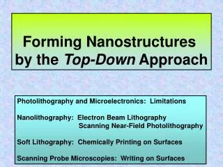
Background • Top-down & Bottom-up Fig. 5 Two approaches to control matter at the nanoscale. [6]
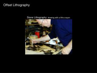
Background • Top-down Techniques: • Bulk-/film-machining • Surface-machining • Mold-machining Fig. 7 Surface-machining [7] Fig. 8 Mold-machining with soft lithography [7] Fig. 6 Bulk-/film-machining [7]
Outline • Introduction • Background • Technology • Lithography Needs to Beat Its Limit • Future Work
? Lithography == Photolithography To describe a lithography imaging system: Resolution (RES) = k1 λ / NA Depth of focus (DOF) = k2 λ / (NA)^2 k1 and k2 are process-related factors, normally ≥ 0.6 According to Rayleigh criteria, theoretical values of k1 and k2 are equal to 0.5 Use shorter wavelength To increase resolution Increase NA Continuous advancement of photolithography In the past decades’ struggle… Proposal and development of other techniques Electron beam lithography, nanoimprint lithography, interferometric lithography, X-ray lithography, extreme ultraviolet lithography, scanning probe lithography… Lithography Needs to Beat Its Limit
Outline • Introduction • Background • Technology • Engineering Tricks with Photolithography • Future Work
Engineering Tricks with Photolithography “Dear old” photolithography technique MUST be saved ! • V-groove Heterostructure Patterning • Double-exposure Patterning • Immersion Lithography
V-groove Heterostructure Patterning E. Kapon et al. Appl. Phys. Lett. 55, 2715 (1989) C. Percival et al. IEEE TRANSACTIONS ON ELECTRON DEVICES, VOL. 47, NO. 9, 2000 K. F. Karlsson et al. Appl. Phys. Lett. 90, 101108 2007
Double-exposure Patterning http://www.imec.be/wwwinter/ mediacenter/en/SR2005/html/ 142319.html develop Shift reticle or 2nd reticle • Use reduced exposure dose (60-80%) • Stepper movement must be controlled precisely (nm) -> piezoelectric element
Immersion Lithography Immersion Lithography Results65nm line-and-space pattern ArF laser with a 1.07 NA imaged these 45-nm features http://www.nikon.co.jp/main/eng/portfolio/about/technology/nikon_technology/immersion_e/index.htm http://oemagazine.com/FromtheMagazine/jul04/underwater.html
Outline • Introduction • Background • Technology • Electron Beam Lithography (EBL) • Future Work
Electron Beam Lithography Use high voltage electrons (1 kV – 100 kV) to transfer nano-patterns into resist (ex. PMMA) on the substrate by directly writing. Resist development Define pattern on spin coated E-beam resist RIE etching Cladding deposition Masaya Notomi and Toshiaki Tamamura http://people.ece.cornell.edu/lipson/nature/fabrication.htm http://www.ee.pdx.edu/~jeske/litho/electronbeamlitho.html
Outline • Introduction • Background • Technology • Nanoimprint Lithography (NIL) • Future Work
Nanoimprint Lithography Photo Nanoimprint Lithography Thermoplastic Nanoimprint lithography http://www.semiconductoronline.com/Content/ProductShowcase/ http://www.nanonex.com/Picture/Resists2.jpg
Outline • Introduction • Background • Technology • Scanning Probe Lithography (SPL) • Future Work
Scanning Probe Lithography Local oxidation (anodization process) mask fabrication and etching to produce quantum wires (a) Starting from a patterned aluminium film (b) “positive” mask (d) “negative” mask (c, e) Reactive ion etching A. Notargiacomo et al., Materials Science and Engineering C 19, 185-188 (2002)
Outline • Introduction • Background • Technology • Summary of Different Lithography Techniques • Future Work
Outline • Introduction • Background • Technology • Future Work
Future Work Figure 1. Two quantum dots connected by a wire behave somewhat like atoms in a molecule, with different energy levels, a property that might be useful as a switch in a quantum computer. ( Arizona State University) from www.aip.org/tip/INPHFA/vol-9/iss-1/p14.html Figure 3. 1 Organic Light Emitting Diodes (OLEDs) for displays 2 Photovoltaic film that converts light into electricity 3 Scratch-proof coated windows that clean themselves with UV 4 Fabrics coated to resist stains and control temperature 5 Intelligent clothing measures pulse and respiration 6 Bucky-tubeframe is light but very strong 7 Hipjoint made from biocompatible materials 8 Nano-particle paint to prevent corrosion 9 Thermo-chromic glass to regulate light 10 Magnetic layers for compact data memory 11 Carbon nanotube fuel cells to power electronics and vehicles 12 Nano-engineered cochlear implant Figure 2. Nano robots From http://www.witn.psu.edu/articles/article.phtml? article_id=41&show_id=7