Download
1 / 36
360 likes | 473 Views
Explore the optical properties of nanostructured materials in this lecture. Topics include photonic crystals, silicon nanocrystals, and applications in optoelectronics and biomedicine.

E N D
Lecture 1 LINEAR OPTICAL EFFECTS IN NANOSTRUCTURED SOLIDS Pavel Kashkarov M.V. Lomonosov Moscow State University, Physics Department Russian Research Center “Kurchatov Institute”
Outline • Introduction • Photonic crystals and anisotropic layers based on porous silicon • Silicon nanocrystals in dielectric matrix for optoelectronic applications • Silicon nanocrystals for biomedical applications • Conclusions
Photonic crystals and anisotropic layers based on porous silicon 1. The idea that nanostructuring of homogenous and isotropic media results in completely new optical properties was suggested many years ago (see excellent textbook “Principles of Optics” by M. Born and E. Wolf). But at that time there was not appropriate technology to fabricate nanostructured materials. 2. There were suggested two types of structures with form anisotropy: parallel layers and periodically arranged nanocylinders. Both structures show a strong birefringence.
Form Birefringence Lord Rayleigh
...Photonic crystals and anisotropic layers based on porous silicon • Only recently an electrochemical technique was applied to fabricate such structures on semiconductor substrate (mainly silicon). • Another type of an artificial medium is a photonic crystal. It turns out that it also can be easily made by the electrochemical treatment of semiconductors. • The obvious advantage of porous nanostructured media is the possibility to change the optical properties of the sample by filling pores by different gaseous, liquid and solid substances.
Electrochemical nanostucturing of semiconductors HF solution c-Si
microporous mesoporous (100) surface, =10 cm (110) surface,=3 mcm Different morphologies of porous silicon Preferential pore growth in <100> crystallographyc direction
Tailoring of the Refractive Index by Nanostucturing Effective media approximation (Bruggeman model ) • eff of the disordered heterogeneous mixture: where P is porosity refractive index:
Porous Silicon Based Photonic Crystals Ideal Bragg reflector 12 pairs n1=1.3, n2=2 Bragg condition: n1d1+n2d2=/2
1D Photonic Crystal Based onPorous Silicon n2 d2 n1 d1
Linear Optical Properties of Photonic CrystalsBased onPorous Silicon
Strong Optical Anisotropy in (110) Porous Silicon Generalized Bruggeman model
Effect of Porosity on Birefringence of Nanostructured Silicon Films For layers prepared at j =100 mA/cm2 : Δn=0.24 <n> = (no+ne)/2 = 1.3 δn=Δn/<n> = 0.18 Nanostructured Si films have large birefringence value δn =18%
Polarization Tunable Photonic Crystals Reflection spectra
Oxidized Porous Silicon X-ray diffraction • Thermal oxidation of birefringent por-Si film results in formation of chemically stable, transparent for visible radiation medium, which possesses optical anisotropy. Oxydized por-Si c-Si Por-Si
Birefringence of Oxidized Porous Silicon 950 oC 2.5 h Transparent birefringent film Oxidized por-Si film on a mirror under a polarizer. In oxidized por-Si birefringence is 2 times higher than in quartz
Silicon nanocrystals in dielectric matrix for optoelectronic applications • Silicon was, is and will be the main material for microelectronics, but application of silicon in optoelectronics is limited. • Low probability of radiative electron transition in Si can be increased by formation of nanoparticles or/and by an introduction of activators of luminescence. • A Er3+ ion possesses rather promising properties as a luminescence activator in Si. The Er3+ luminescence line (λ=1.54µm) corresponds to a maximum of transmission in the quartz fiber waveguides. • For formation of light emitting device we combined both approaches
Light absorption in semiconductors (interband transitions) Е GaAs L Eg=1.52эВ <111> <000> <100> Е f h Eg Eg 0– i 0 • Direct gap materials (GaAs, InP, CdTe, CdS )
where d is a nanoparticle size Light absorption in semiconductors (interband transitions) • Indirect gap materials (Ge, Si, GaP ) • Heisenberg uncertainty principle
Quantum size effect 2D structure Quantum size effect enables one to modify absorption and luminescence spectra of semiconductor nanoparticles The effect becomes appreciable when the size of a particle is less then 10 nm
Er Size-controlled Si nanocrystals in nc-Si/SiO2 Superlattices 3nm Preparation Details: Alternating evaporation of SiO powder in vacuum 10-7 mbar or in oxygen atmosphere underoxygen partial pressure of 10-4 mbar. This changes the stoichiometry x of SiOx alternatively between 1 and 2. 2. SiO/SiO2 superlatticies are characterized by the thickness of the SiO layers varied between 1 and 3 nm and the thickness of SiO2 layers between 2 and 3 nm. The number of periods varied between 30and 90. 3. The evaporated samples were annealed at 1100 oC under N2 atmosphere. Thus nc-Si/ SiO2 superlattices were obtained. 4. Er doped nc-Si/SiO2 superlattice were produced by implantation with Er ions (energy 300 keV, doses 1014 – 5·1016 cm-2) followed by TA at 900 oC for 5-60 minutes. M. Zacharias et al., APL 80, 661 (2002).
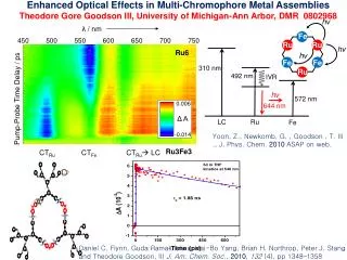
Size Dependent PL of nc-Si/SiO2 Structures • Size of Si nanocrystals is controlled by initial thickness of SiO layer in SiO/SiO2 superlattice • The peak position of PL spectrum is determined by quantum confinement and excitonic effects in Si nanocrystals in SiO2 matrix.
Er3+ Effect of Er doping on PL of nc-Si/SiO2 1.5 mm (0.8 eV) P.K.Kashkarov et al., JETP 64,1123 (2003) • Er doping results in both two order of magnitude quenching of the exciton PL and a strong emission line at 1.5 m • Er-doped a-SiO2 layers does not exhibit efficient Er photoluminescence • Efficient energy transfer from electronic excitation of Si nanocrystals to Er ions
N1 N0 Transient PL Investigation of Er3+ Population Inversion • Lifetime of Er-related PL becomes shorter at Iexc > 0.1 W/cm2 that correlates with the population inversion of Er3+
Silicon nanocrystals for biomedical applications • Oxygen molecules exist in several forms: non-active one (ground state) and active ones (excited states) • In the active form oxygen is toxic and therefore fatal for any live cells • This property of active oxygen is used to clean water containing harmful microbes and is the base of our immunity • In some cases generation of active oxygen can be applied for cancer therapy • But how an oxygen molecule can be transferred into active form?
Electronic Structure of Molecular Oxygen 1S t = 7 s • Excited States: • Spin Singlet • Energy-rich • High chemical Reactivity: • S(O2) + S(Mol.) S(Mol.) 1.63 eV 1D t = 50 min 0.98 eV • Ground State: • Spin Triplet • Paramagnetic • Chemically inert: • T(O2) + S(Mol.) S(Mol.) 3S O O Optical Excitation is inefficient Photosensitizer is required
Energy Transfer S1 T0 S S0 T R Donor Acceptor Photosensitization: Basic Principle • Efficient Energy Transfer requires: • Small Spatial Separation between Donor and Acceptor • Spectral Overlap of Donor and Acceptor Energy Bands • High Quantum Efficiency of Donor Luminescence
Si Nanocrystal Assemblies as Photosensitizers? • Simple Electrochemical Preparation • Open Nanostructure • Efficient Photolumenescence A.G.Cullis and L.T.Canham, Nature 353, 335 (1991) • Broad Tunable Emission Band • Long Exciton Lifetime (µs - ms)
Effect of Physisorbed Oxygen Molecules on PL of Si Nanocrystal Assembly • PL Quenching of • Excitonic and Defect • Emission Band • 1D 3S Emission Line • of 1O2 Evidence for Energy Transfer from Excitons to O2
Singlet Oxygen Photosensitization in Water 1 mg of nano-Si (from micropor-Si) dispersed in 3 ml of H2O for tSO~ 1-3 ms: NSO ~ 1015 – 1016 (1/cm3)
Effect of Porous Si on cancer cells (in vitro experiments with mouse fibroblasts) Cells were counted by using optical density measurements Cancer cell number vs porous Si concentration in the dark (blue symbols) and after illumination (red symbols)
DNA Analysis Histogram of DNA content for the cancer cells kept in the nutrient solution with dispersed porous Si (1.5 g/l) in darkness (blue curve) and after illumination (red curve). Symbols G1, S, and G2 mark different cycles of the cell proliferation. The apoptotic cell region is marked by A. Inset shows the relative contribution of G1, S and G2 regions vs nc-Si concentration in the dark (blue symbols) and after illumination (red symbols)
tumour Si Si Si Si Si Si Si Si Si Si Si Si Si Si Si Photodynamic cancer therapy h triplet 3О2 nc-Si nc-Si singlet1О2 nc-Si
General Conclusions • Nanostructuring of homogenous and isotropic Si-crystals enables one to form photonic media with unique properties • Ensembles of Si-nanocrystals in a dielectric matrix are promising base for silicon laser compatible with microelectronic technology • Bio-compatible Si-nanoparticles are effective photosensitizers of singlet oxygen generation what can be applied for photodynamic cancer therapy