Field Programmable Gate Array
Field Programmable Gate Array. FPGA. 8 x 1 ROM (LUT). Using ROM as Combinational Logic. B. C. F. A. C. A. B. C. F. LUT (B+C). LUT A’f1 + Af2. Mapping Larger Functions To ROMs. LUT (CD). B. C. D. f1. f2. F. B. C. D. A.

Field Programmable Gate Array
E N D
Presentation Transcript
Field Programmable Gate Array FPGA ECEn 224
8 x 1ROM (LUT) Using ROM as Combinational Logic B C F A C A B C F ECEn 224
LUT(B+C) LUTA’f1 + Af2 Mapping Larger Functions To ROMs LUT(CD) B C D f1 f2 F B C D A Very similar to how we decomposed functions to implement with MUX blocks… ECEn 224
ROM vs. LUT • A ROM can be used as a lookup table (LUT) • An FPGA contains many, many such LUTs • Possibly hundreds of thousands • A 3LUT has 3 inputs and 1 output • A 4LUT has 4 inputs and 1 output • 4LUTs are the most common… ECEn 224
Mapping a Gate Network to LUTs ECEn 224
Mapping a Gate Network to 3LUTs 3LUT #2 3LUT #1 3LUT #3 ECEn 224
Mapping Same Network to 4LUTs 4LUT #2 4LUT #1 ECEn 224
Mapping Equations to LUTs • How many 4LUTs do the following functions require? F = a F = abcd F = a’b’c’d + a’bcd’ + a’b’c’d’ + a’b’cd F = a + b + c + d F = (a +b + c + d)(a’ + b’ + c’ + d’) • Each equation requires a single 4LUT! Number of LUTs isn’t a function of equation complexity,but a function of number of unique inputs ECEn 224
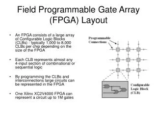
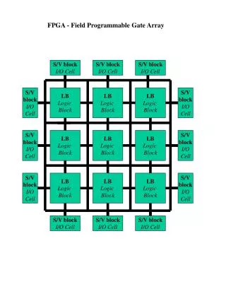
FPGAs – What Are They? Programmable Logic Elements(LEs) Programmable wiring areas I/O Buffers I/O Buffers I/O Buffers I/O Buffers communicatebetween FPGA andthe outside world I/O Buffers An FPGA is a Programmable Logic Device (PLD)It can be programmed to perform any function desired. ECEn 224
D Q 0 1 Programmable Logic Elements (LEs) • Typically contain a LUT, wires, and storage inA 4LUT out inB inC inD 16 clk ECEn 224
D Q 0 1 Programmable Logic Elements (LEs) • Typically contain a LUT, wires, and storage inA 4LUT out inB inC inD 16 clk This mux provides a registered or unregistered function of the 4 input variables ECEn 224
D Q 0 1 Programmable Logic Elements (LEs) • Typically contain a LUT, wires, and storage inA 4LUT out inB inC inD 16 clk Black dots indicate programming bits(configuration bits) ECEn 224
D Q 0 1 Programmable Logic Elements (LEs) • Typically contain a LUT, wires, and storage inA 4LUT out inB inC inD 16 clk On power up, configuration bits are loaded into FPGA This customizes its operation (LUT function, MUX selection) ECEn 224
D Q 0 1 Programmable Logic Elements (LEs) • Typically contain a LUT, wires, and storage inA 4LUT out inB inC inD 16 clk Typically, configuration bits are not changed during circuit operation (but, some FPGA’s are dynamically reconfigurable) ECEn 224
D Q 0 1 0 1 Another LE Structure • Provides two outputs • One combinational, one registered inA inB 4LUT outReg inC inD inE clk 16 outComb ECEn 224
D Q 0 1 0 1 One Configuration inA inB 4LUT outR = reg(inB(inC+inD)) inC inD inE =1 clk 16 fn=inB(inC+inD) ECEn 224
D Q 0 1 0 1 Another Configuration inA inB 4LUT outR = reg(inA) inC inD inE =0 clk 16 fn=inC’ outC = inC’ =1 ECEn 224
D Q 0 1 0 1 Yet Another Configuration inA inB 4LUT outR = reg(inC’) inC inD inE =1 clk 16 fn=inC’ outC = inC’ =1 ECEn 224
D Q 0 1 An LE With Carry/Cascade Logic Cout inA 4LUT Carry/Cascade out inB inC inD 16 clk Cin Can do two functions at once (Sum and Cout) Carry/cascade logic optimized for add/subtract and wide AND,OR, … Cin and Cout have dedicated connections to neighboringLEs fast carry chains fast arithmetic ECEn 224
Logic Elements An FPGA Architecture (Island Style) Column Wires Row wires Each LE is configured to do a function Wire intersections are programmed to either connect or not ECEn 224
Programmable Interconnect Junction Column wire ON Connected =1 Row wire Unconnected OFF =0 ECEn 224
Example Problem • Generate the N, Z, P status flags for a 6-bit microprocessor Z’ Z N P D5 D0-D5 N’ ECEn 224
Example Problem • Generate the N, Z, P status flags for a 6-bit microprocessor Z’ Z N P D5 D0-D5 N’ Can be done with wiring only or with 1 4LUT Will require 2 4LUTs Will require 1 4LUT ECEn 224
N 1 2 3 4 5 D0 D1 6 7 8 9 10 P D2 11 12 13 14 15 D3 D4 D5 Z LUT #1: F1 = D0’• D1’• D2’• D3’LUT #8: F3 = D5 N output LUT #7: F2 = F1•D4’•D5’ Z outputLUT #9: F4 = Z’ • N’ P output ECEn 224
N 1 2 3 4 5 D0 D1 6 7 8 9 10 P D2 11 12 13 14 15 D3 D4 D5 Z LUT #1: F1 = D0’• D1’• D2’• D3’LUT #8: F3 = D5 N output LUT #7: F2 = F1•D4’•D5’ Z outputLUT #9: F4 = Z’ • N’ P output ECEn 224
N 1 2 3 4 5 D0 D1 6 7 8 9 10 P D2 11 12 13 14 15 D3 D4 D5 Z LUT #1: F1 = D0’• D1’• D2’• D3’LUT #8: F3 = D5 N output LUT #7: F2 = F1•D4’•D5’ Z outputLUT #9: F4 = Z’ • N’ P output ECEn 224
N 1 2 3 4 5 D0 D1 6 7 8 9 10 P D2 11 12 13 14 15 D3 D4 D5 Z LUT #1: F1 = D0’• D1’• D2’• D3’LUT #8: F3 = D5 N output LUT #7: F2 = F1•D4’•D5’ Z outputLUT #9: F4 = Z’ • N’ P output ECEn 224
N 1 2 3 4 5 D0 D1 6 7 8 9 10 P D2 11 12 13 14 15 D3 D4 D5 Z LUT #1: F1 = D0’• D1’• D2’• D3’LUT #8: F3 = D5 N output LUT #7: F2 = F1•D4’•D5’ Z outputLUT #9: F4 = Z’ • N’ P output ECEn 224
Configuring an FPGA • Most FPGAs have a configuration input pin • Configuration bits are shifted into FPGA using this pin, one bit per cycle • Configuration bits in FPGA linked into a long shift register (SIPO) • Examples on following slides are conceptual • Commercial devices slightly different ECEn 224
Structure of a 3LUT b0 b1 b2 ConfigurationStorage Bits (Flip Flops) b3 LUT Output b4 b5 b6 It’s just an 8:1 MUX LUT inputs select which configbit is sent to LUT output Programming LUT function setting configuration bits b7 3 LUT Inputs ECEn 224
D Q D Q 0 1 0 1 B6 CONFIG CCLK How are the Configuration Bit Flip Flops Loaded? A serial-in/parallel-out(SIPO) shift register These are the configuration bitswhich the LUT selects from … B7 CONFIG CCLK … ECEn 224
Configuring the Programmable Interconnect Column wire Configuration bit b Also arranged in a SIPO shift register Row wire ECEn 224
Additional FPGA Features Found in commercial FPGAs ECEn 224
Configurable Input/Output • I/O blocks allow internal FPGA signals to connect to external pins • Configurable I/O block features: • Can be configured as inputs or outputs • Electrostatic discharge (ESD) protection • Input signal conditioning (voltage levels, …) • Output drive • Fast, slow • Strong, weak • Tri-state • Handles a variety of electrical standards • LVTTL • LVCMOS • PCI • LVDS • … • I/O blocks are configured when the rest of the chip is configured ECEn 224
Configuration Storage • Actual configuration storage is not flip flops • Many use SRAM memory cells • Different technologies • Program once • Fuse, anti-fuse configuration • Program multiple times • SRAM-based configuration • Some chips can be partially reconfigured, even while rest of chip is running ECEn 224
Programmable Interconnections • Expensive to put programmable connections at every wire junction • Commercial parts use partially populated junctions • Little or no loss of routing flexibility ECEn 224
Hierarchical Routing • Collection of short, medium, and long wires • Both rows and columns • Signals use wires that go distance needed • CAD tools make determinations • Like alleys, streets, expressways in a city • Longer distance more limited access points ECEn 224
Clustered LE’s • Cluster: >= 1 LE • Example: Cluster of 4 • Dedicated wires within groups of 4 LE’s • Closely related to hierarchical routing • Higher performance • Different vendors different clustering ECEn 224
Embedded Function Units • Place the following into the FPGA fabric:Multipliers Memories (Block RAM) I/O interfaces (e.g. gigabit serial links or Ethernet PHY/MAC) CPU’s (PowerPC, ARM, …) • Result: higher speed, higher density, lower power designs ECEn 224
FPGAs Compared To Other Technologies ECEn 224
Performance vs. Flexibility CPUs & DSPs FPGAs Flexibility ASICs Performance ASIC = Application Specific Integrated Circuit Goal: the performance of ASIC’s with the flexibility of programmable processors. ECEn 224
FPGAs vs. CPUsFlexibility • Any function can be programmed to run on a CPU • Programming is relatively simple to do • Any function can also be configured onto an FPGA • Design is much more difficult and time consuming since it’s a digital logic design • “Hardware is harder than software” • Both CPUs and FPGAs can be reprogrammed (reconfigured) in the field • The winner: CPUs ECEn 224
FPGAs vs. CPUs Performance • 10+ years of research 10x-100x performance advantage for FPGAs! • Custom hardware • No fetch, decode, or memory access overhead • Significant parallelism (e.g., pipelining) • Case in point: 1998 SONAR beamformer on an FPGA • BYU Configurable Computing Lab research • 2 x 10⁹ FLOP/sec sustained • 10x-80x faster than comparable CPU technology • The winner: FPGAs ECEn 224
FPGAs vs. ASICsFlexibility • ASIC is a static hardware design • Wires and transistors fixed at manufacture time • Cannot be upgraded (reprogrammed) in the field • FPGA can be configured (and reconfigured) • FPGA platform used for a variety of applications • CCM = Custom Computing Machine (based on FPGAs) • The winner: FPGAs ECEn 224
FPGAs vs. ASICsPerformance • Both ASICs and FPGAs are custom hardware designs • FPGA configurability comes at great cost • FPGA density is much lower than that of an ASIC • Low density means logic must be physically spread out • Result: • FPGAs are slower, physically larger, and more power hungry than a custom ASIC chip • For some/many applications FPGAs may… • …be too slow • ...not hold enough logic • …be too power hungry • The winner: ASICs ECEn 224
FPGAs vs. ASICsCost • Once the design is complete: • FPGAs can be purchased off-the-shelf and programmed in seconds • Negligible up-front costs • Inexpensive for small volume • Per part cost is high • ASICs require time-consuming, expensive manufacturing process • Fabrication facility (> $1 billion) • Significant up-front costs • Expensive for small volume • Per part cost is very low, when volume is high • The winner: Depends on volume and application! ECEn 224
FPGA Non-recurring engineering (NRE) costs = $0 Per-part cost = $20(prices vary from a few $’s to $1000’s) Cost to produce 100 = $2K Cost to produce 106 = $20M ASIC NRE costs = $5M Per-part cost = $1 Cost to produce 100 = $5M + $100 ≈ $5M Cost to produce 106 = $5M + $1M = $6M FPGA vs. ASIC Production Cost Example Volume produced makes a big difference! ECEn 224
FPGAs vs. ASICsTime to Market and Bug Fixes • Manufacturing Time • Shorter time to market makes money sooner • FPGA = seconds to configure • ASIC = weeks to months • Fixing Bugs • FPGA = modify design + reconfigure FPGA • Reconfigurability can make debugging easier • ASIC = modify design + remanufacture • The winner: FPGA ECEn 224
FPGAs vs. ASICs - Summary • Two very different technologies • Flexibility: FPGA wins • Performance: ASIC wins • Risk: ? • Cost: ? • Complex Decision • Only partially based on technical issues • Significant business issues • Cost • Risk • Time-to-market • Market characteristics (elasticity, price sensitivity, …) ECEn 224
Design for FPGAs • Draw schematics or write HDL • CAD toolmaps design to LUTs + FFs • CAD tool generates bitstream • Load bitstream to configure the FPGA ECEn 224