Download

1 / 18
200 likes | 327 Views
This work discusses the design and optimization of a first-order column-level Delta-Sigma ADC for CMOS image sensors to minimize power consumption and area usage, achieving high SNR and performance. It presents the structure, modulator, operational transconductance amplifier, decimator design, simulation results, and conclusions.

E N D
Optimization of Delta-Sigma ADC for Column-Level Data Conversion in CMOS Image Sensors Alireza Mahmoodi and Dileepan Joseph University of Alberta, Canada Email: mahmoodi@ualberta.ca, dil.joseph@ualberta.ca
Outline • Problem • Solution (optimized delta-sigma ADC) • ADC structure in image sensors • Design and optimization of ADC • ADC simulation and performance evaluation • Conclusion
Problem Lower supply voltage Smaller dynamic range CMOS technology scales down Lower the achievable SNR More nonlinear analog circuits
Solution (delta-sigma ADC) • Unlike Nyquist rate ADCs, oversampled ADCs (delta-sigma ADC) can filter the temporal noise in array sensors, achieving higher SNR. • Delta-sigma ADC is very tolerant to nonidealities of CMOS circuits. • Flexibility of trading the number of bits-per-pixel, with the frame rate in delta-sigma ADC is another advantage. • A few works have designed the DS-ADC for column or pixel level but with large power and area usage. • Main issue of DS-ADC is power consumption and area usage which should be minimized (subject of this work).
ADC structure in image sensors • Chip level ADC (One ADC for all of the pixels) • High spatial resolution • But, high noise, high power, fast ADC is needed, • Pixel level ADC (One ADC for each pixel or group of pixels) • Low noise, low speed ADC is needed, low power • But, low spatial resolution, high FPN. • Column level ADC (One ADC for each column or group of columns) • A compromise between pixel level and chip level. In this work a first-order column-level delta-sigma ADC will be designed.
Why first order? Using first order structure • Main concern was minimization of power and area. Less sensitive to gain error of the integrator due to the capacitor mismatch Higher oversampling ratio is needed Small area because of simple structure More KT/C noise will be filtered Smaller capacitors could be used Comparing to higher order structures, low power and smaller area could be achieved
Modulator of first order structure • The analog parts must be carefully designed because their nonidealities may limit the overall ADC performance.
Specificationsof the modulator • Mismatch is not the limiting factor. • So, the minimum value for the capacitors in the integrator is determined by KTC noise. • The minimum value for Capacitors were determined. • Then, other parameters were designed.
Operational Transconductance Amplifier • OTA is the most critical Component • Folded-cascode OTA structure with gain boosting was used.
DDA-CMFB circuit. • OTA needs a common-mode feedback (CMFB) circuit . (1) Switched capacitor CMFB • It has large swing and linearity. • Loads the output of the OTA, reducing its UGB and SLR.Large area is needed (2) We used a differential-difference amplifier CMFB (DDA-CMFB). • It can offer enough swing and linearity with very small area.
Decimator design • The coefficients of the decimation filter are generated at the chip level. • The decimation filter is only an accumulator at the column level which consumes 60μW power.
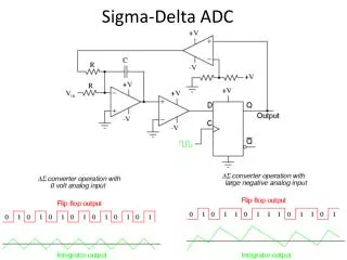
Simulation results • Simulation was done for a 0.18μm CMOS process using Cadence and Simulink. • SNR versus OSR based on: (a) Theoretical calculation (b) Simulink using 5000 samples (c) Simulink using 50 samples (d) Cadence (modulator) and Simulink (decimator) using 50 samples
Performance evaluation • Figure-of-merit (FM) is defined as
Conclusion • The design of a first-order delta-sigma ADC for column level data conversion in an image sensor has been presented. • Since the first-order modulator is not sensitive to gain error due to capacitor mismatch, minimum-size capacitors may be used to minimize the power consumption and area usage. • A new structure for decimator was introduced. • The proposed ADC has a low power consumption of 210μW. • Simulation results are very close to the theoretical values • Presently, the design is being laid out in a 0.18μm process. Ultimately, the design will be fabricated and tested.
Acknowledgements • This work was sponsored by the Natural Sciences and Engineering Research Council of Canada and the Mary Louise Imrie Award.
References • [1] J. Fortier, N.G. Tarr, A. Swaminathan, and C. Plett, “1.2 v 0.18 um cmos imager with column-level oversampling,” in Solid-State Circuits Conference, 2001. ESSCIRC 2001. Proceedings of the 27th European,18-20 Sept. 2001, pp. 105–108. • [2] A. El Gamal and H. Eltoukhy, “Cmos image sensors,” Circuits and Devices Magazine, IEEE, vol. 21, no. 3, pp. 6–20, May-June 2005. • [3] D. Joseph and S. Collins, “Modeling, calibration, and correction of nonlinear illumination-dependent fixed pattern noise in logarithmic cmos image sensors,” Instrumentation and Measurement, IEEE Transactions on, vol. 51, no. 5, pp. 996–1001, Oct. 2002. • [4] S.R. Norsworthy, R. Schreier, and G.C. Temes, Eds., Delta-sigma datatheory • design and simulation, IEEE Press, 1997. • [5] J. Candy, Y. Ching, and D. Alexander, “Using triangularly weighted interpolation to get 13-bit pcm from a sigma-delta modulator,” Communications, IEEE Transactions on [legacy, pre - 1988], vol. 24, no. 11, pp. 1268–1275, Nov 1976. • [6] B.E. Boser and B.A. Wooley, “The design of sigma-delta modulation analog-to-digital converters,” Solid-State Circuits, IEEE Journal of, vol. 23, no. 6, pp. 1298–1308, Dec. 1988. • [7] H. Zare-Hoseini, I. Kale, and O. Shoaei, “Modeling of switchedcapacitor delta-sigma modulators in simulink,” Instrumentation and Measurement, IEEE Transactions on, vol. 54, no. 4, pp. 1646–1654,Aug. 2005. • [8] B. Razavi, Design of Analog CMOS Integrated Circuits, McGraw-Hill Inc., 2000. • [9] L. Luh, J. Choma Jr., and J. Draper, “A continuous-time common-mode feedback circuit (cmfb) for high-impedance current mode application,” in Electronics, Circuits and Systems, 1998 IEEE International Conference on, 7-10 Sept. 1998, vol. 3, pp. 347–350. • [10] M. Safi-Harb and G.W. Roberts, “Low power delta-sigma modulator for adsl applications in a low-voltage cmos technology,” Circuits and Systems I: Regular Papers, IEEE Transactions on [see also Circuits and Systems I: Fundamental Theory and Applications, IEEE Transactions on], vol. 52, no. 10, pp. 2075–2089, Oct. 2005.