Download

1 / 4
0 likes | 18 Views
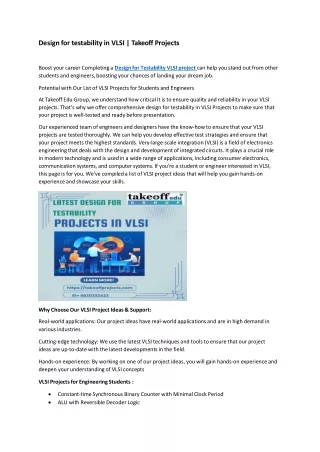
Takshila-vlsi.com design course in Bangalore enables you to unlock the potential of testability. Improve your career and abilities with the assistance of our professional advice.

E N D
Design For Testability Course In Bangalore | Takshila-vlsi.com Takshila-vlsi.com design course in Bangalore enables you to unlock the potential of testability. Improve your career and abilities with the assistance of our professional advice. design for testability course in bangalore
About Us: - Online Analog Layout Design / Online Custom Layout Design / Online IC Layout Design course mainly focused on giving hands-on practical exposure in doing chip layout design for a given analog & mixed signal design. By end of the course you will learn to work in Linux environment, schematic entry in EDA tool, placement planning, analog and digital layout design, routing and physical verification checks like DRC, LVS for typical analog circuits such as Opamp, PLL, Bandgap, LDO and standard cells. You will also understand fixing deep sub-micron process issues like Antenna, Latchup, EM&IR. Our design for test training is designed by the best experts according to the most trending industry requirements. Our students are given several hands-on projects that are based on ATPG, MBIST, SCAN, as well as JTAG. This is to ensure that they turn out to be the best DFT engineers that they can be thus establishing their place in the industry quite fast after they have completed their studies. That is what makes us one of the best design for test training institutes in India.
Takshila Institute of VLSI Technologies 39/4, 2nd Floor, Kishan Arcade, erns City Road Mahadevapura,Bengaluru Karnataka 560048 India 9742972744 Contact us:-