Design for Testability
Design for Testability. 陳正斌 (03)5773693#157 jbchen@cic.org.tw. Agenda. Logic Testing Basic Concept Design for Testability RTL Rule Checker DFT Guidelines and Rules Synopsys DFT Design Flow Memory Testing Basic Concept Memory BIST SynTest SRAMBIST Flow.

Design for Testability
E N D
Presentation Transcript
Design for Testability 陳正斌 (03)5773693#157 jbchen@cic.org.tw
Agenda • Logic Testing • Basic Concept • Design for Testability • RTL Rule Checker • DFT Guidelines and Rules • Synopsys DFT Design Flow • Memory Testing • Basic Concept • Memory BIST • SynTest SRAMBIST Flow
Apply Input (Stimulus) Compare Output (Response) What is Testing • Testing is a process of determining whether a device is good (function correctly) or not • Testing includes test pattern generation, application and output evaluation Test Pattern DUT
Defect detected during field testing Defect detected during system testing Defect detected during IC testing Why Testing • In order to guarantee the product quality, reliability, performances, etc. • Cost is the most important. • The rule of ten
Simplified IC Production Flow Specification Layout Design Process Wafer Probe Test Packaging Final Test Marking QA Sample Test Shipping
Verification v.s. Test (1/2) • Design verification ensures “design” matches intent • Manufacturing test ensures “parts” are manufactured correctly • How is manufacturing test performed ? Test Pattern (Test Problem) Fail Tester (ATE) Good Device Under Test (DUT)
Verification v.s. Test (2/2) Design Manufacture Synthesis always @(a or b) begin c = a & b end Verification Test Verification Diagnosis
Automatic Test Equipment • Tester (ATE) • Key features to be aware of • Number of pins • Number of clocks • Frequency • Accuracy • Precision • Number of scan channels • Amount of memory • Vector application formats • … … …
Type of Testing • On Wafer Test • Characterization Test • Production Test • Burn-In Test • Diagnostic Test • … … …
Test Items • Function Test • Verify functionality • Structural Test • Verify manufacturability • Parametric Test • Verify AC and DC parameters • At-Speed Test • Verify performance • Leakage Test • Defects may cause high leakage current
1.E+08 1.E+07 Pentium 486 1.E+06 Transistors 386 1.E+05 286 1.E+04 8080 1.E+03 1998 2002 1994 1970 1974 1978 1982 1986 1990 Year Pins/Gates TTL logic allowed easy access to individual gates. Pins / Gates << 0.001Hard to access to a chip.
What is Fault & Fault Model • Fault is a physical defect in a circuit or system • Fault model is the logical effect of a fault (physical defect) • Reduce the test complexity • Independent of technology
Yield & Fault Coverage • Yield (Y) is the ratio of the number of good dies per wafer to the number of dies per wafer • Y = (# of good dies) / (# of all dies) • Fault coverage (FC) is the measure of the ability of a test set to detect a given class of faults that may occur on the device under test (DUT) • FC = (# of detected faults) / (# of possible faults)
Defect Level & Fault Coverage • Defect level (DL) is the fraction of devices that pass all the tests and are shipped but still contain some faults • DL = 1-Y(1-FC) [Williams and Brown 1981] • Defect level is measured in terms of DPM (detects per million), and typical requirement is less than 200 DPM i.e. 0.02 % DL = 200 DPM
Board Failing Probability (%) Chip Defect Level (DPM) Y = 50% Y = 90% 10,000 1,000 100 10 99 99.99 99.9 90 Fault Coverage Defect Level (DPM) Data Source: Prof. Ed. McCluskey 1988, 1998 Defect Level & Quality • High fault coverage minimizes DPM • High fault coverage is imperative when yield is low
The Testing Problem • Given a set of faults in a device under test (DUT), how to obtain a small number of test patterns which detects high fault coverage ? • What faults to test ? (fault modeling) • How are the test patterns obtained ? (test pattern generation) • How is the test quality (fault coverage) measure ? (fault simulation) • How are test patterns applied and results evaluated ? (ATE/BIST)
Fault Model (1/3) • Single stuck-at fault • A line (gate input/output) in the circuit is fixed at logic 0 or logic 1 and independent of other signal values
Fault Model (2/3) • Multiple stuck-at fault • several stuck-at faults occur at the same time • Bridging fault • Two or more normally distinct adjacent lines are shorted together • Other fault models • Single stuck-at fault is the most popular • reduce the complexity of testing • single stuck-at fault cover a lot of multiple stuck-at fault
Fault Simulation (1/2) • To evaluate the quality of a test set • i.e. to compute its fault coverage • Reduce the time of test pattern generation • A pattern usually detected multiple faults • Fault simulation is used to compute the faults accidentally detected by a particular pattern • To generate fault dictionary • For post test diagnosis • To analyze the reliability of a circuit
Fault-free Circuit A B D C Fault Simulation (2/2) Patterns (Sequences) (Vectors) Faulty Circuit #1 (B/0) Response Comparison A B D C Detected? Primary Inputs (PIs) Primary Outputs (POs)
Test Pattern Generation • TA/0={10}, TA/1={00} • TB/0={01}, TB/1={00} • TY/0={01}or{10}or{11},TY/1={00} • T= {00,01,10}
Fault Coverage (Example) Test Pattern (A,B) Faults Detected FC {(0,0)} A/1, B/1, Y/1 3/6= 50% {(0,1)} B/0, Y/0 2/6=33.33% {(1,1)} Y/0 1/6=16.67% {(0,0),(0,1),(1,0)} all 6/6= 100% Functional test need four pattern => reduce test cost
D C B A SA0 Z Test Pattern Generation (1/5) • Path-oriented Techniques • D-algorithm • Step 1. Target a specific stuck at fault
D C B A SA0 / 0 1 Z Test Pattern Generation (2/5) • Fault activate • Step 2. Drive the fault site opposite value • D: 1/0 • D’: 0/1 D
D C B A SA0 0 / 0 1 Z Test Pattern Generation (3/5) • Back tracing (controllability) • Step 3. Specify inputs value to generate the appropriate value at fault site D
D C B A 1 1/0 SA0 0 / 0 1 Z Test Pattern Generation (4/5) • Fault propagation (observability) • Step 4. Select a path from the fault site to the primary output D D’ 0/1 D
D C B A 1 1/0 SA0 0 / 0 1 Z 0/1 1 1 X Discrepancy Test Pattern T Test Pattern Generation (5/5) • Line justification • Step 5. specify all other inputs • Fault detection • If Z(T)faulty differs from Z(T)good D D’ D
Automatic Test Pattern Generation • Goal • Generate the test patterns for target fault model and keep the number of test pattern as small as possible • How ? • Computer-Aided-Design Tools
A/1 Y/1 B/1 Fault Equivalence • A set of faults is equivalent if no test pattern exists to tell them apart. • The function under these faults is equivalent for any input combination
A/0 Y/0 B/0 Fault Collapsing • By testing for only one fault per equivalence set, we can greatly reduce (or collapse) the fault universe • Speed up fault simulation Y/1
a b a c F b c f s-a-0 0 0 1 1 Untestable fault • A fault cannot be excited and/or propagated • Untestable fault is caused by a redundant design of the DUT, that is the line and the associate gate can be removed without changing the logic function of the DUT • Untestable fault is also called as redundant fault • F=ab+a’b+bc • F=ab+a’b
SA0 occurs at here Observe/Verify output at PO 1 0 1 0 Apply test input at PI and set value here to test SA0 Sequence Logic is Harder to Test • Testing requires a sequence of test vectors • Requires initialization of the machine, which may be difficult • Long initialization sequence • Invalid state justification • Faults may cause increasing of internal states
Primary inputs Primary inputs Combinational Logic Combinational Logic Pseudo- PI’s Pseudo- PO’s Primary outputs Primary outputs F/F present state next state Sequential circuit model A single time-frame Sequence ATPG • Time-frame Expansion Cost Issue: For large sequential logic blocks with complexcircuits, sequential ATPG is just not practical.
Design for Testability (1/2) • The design technologies which make test generation and diagnosis easier • Testability = controllability + observability • DFT Methods • Ad-hoc methods • Scan, full and partial • Built-In Self-Test (BIST) • Boundary scan
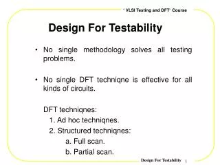
Design for Testability (2/2) • No single DFT technique solves all VLSI testing problems • No single DFT technique is effective for all kinds of circuits • No DFT approach is free • Manpower and tool costs • Area overhead and performance penalty
Scan Design (1/2) • Provide controllability and observability at internal flip-flops for testing • Method • Add scan enable control signal(s) to circuit • Connect flip-flops to form shift registers in test mode • Make inputs/outputs of the flip-flops in the shift register controllable and observable • Types • Internal scan • Full scan • Partial scan • Boundary scan
Primary Input Primary Output Combinational Logic Mode Switch (normal or test) scan_en Scan In FF FF FF Scan Out Scan Design (2/2) • scan_en=1, shift in the scan pattern (clk trig.) • scan_en=0, apply pattern in PI, CL evaluates the response (clk not trig.) • scan_en=0, observe the PO (clk not trig.) • scan_en=0, capture the response (clk trig. once) first scan out • scan_en=1, shift out response (clk trig.)
Non-Scan Register Impact of Scan Design If you plan to insert internal scan, you must account for the impact of scan registers on a chip early in the design flow! Larger area than non-scan registers; (Area overhead) Larger setup time requirement. (Timing impact) TI 1 TI 1 DO DI 0 0 DI TE CLK CLK Multiplexed Scan Register Chain Additional pin overhead
Why DFT ? • Product quality • Reduce field returns (Defect Level) • Improve yield • Test cost • Reduce the complexity of test generation • Reduce the cost of testing
DFT Tools • Synopsys • LEDA • DFT Compiler • TetraMAX • BSD Compiler • SynTest • TurboCheck-RTL • TurboCheck-Gate • TurboScan • TurboBSD • TurboFault • Mentor • DFTAdvisor • FastScan • BSDArchitect • LBISTArchitect
Why RTL Rule Checker? • Motivation • Early identification of RTL design errors. • Reusability of RTL code. • Testability of RTL code. • Fast iteration process
Synopsys LEDA • Features • Check for syntatic/semantic, coding style for synthesis • DFT rules check • RMM rules check • Many Synopsys tools (DC,VCS,Formality ……) • Report the file name and line number of problematic code • Support User defined rule
SynTest TurboCheck-RTL • Features • Lint capability ( more than 400 rules) • Check for syntatic/semantic, coding style for synthesis • DFT rules check (more than 40 rules) • RMM rules check • Report the file name and line number of problematic code • Support User defined rule