1 / 5
50 likes | 58 Views
The semiconductor chip bonding report analyzes emerging technologies, innovative solutions in the area of sub-micron die bonders. The chip bonding report also sheds light on key players, startups and market trends. For more info visit us at https://signicent.com/semiconductor-chip-bonding-report/

E N D
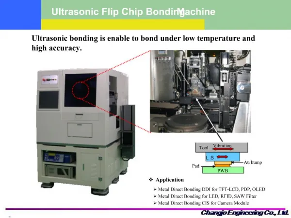
2/7/22, 4:47 PM Semiconductor Chip Bonding Report: How Sub-Micron Die Bonders are Unveiling Market? - Signicent LLP Search... Signicent - Technology, IP & Market Research TRANSFORMING INNOVATION INTO VALUE Signicent LLP (USA & IND) is a well-established consultancy ?rm with 80+ experts that assist businesses globally in their technology, innovation, patents, trademarks, valuation, licensing, tech-transfer & market research needs. in Electronics, eStore, Semiconductor Semiconductor Chip Bonding Report: How Sub-Micron Die Bonders are Unveiling Market? The semiconductor chip bonding report analyzes emerging technologies, innovative solutions in the area of sub-micron die bonders. The chip bonding report also sheds light on key players, startups and market trends. Get in Touch Signicent LLP (USA & IND) info [at] signicent.com Download Report Request Study Proposal Contact Signicent USA: +1-678-648-1313 | UK: +44-121-288- 1313 | INDIA: +91-7696-887-888 Die Bonding is the process of attaching the semiconductor die (or chip) either to its package or to some substrate. The process was originally introduced commercially by IBM in the 1960s for individual transistors and diodes packaged for use in their mainframe systems. Submit an Enquiry Your Name The Chip Bonding Report explain the process to accomplish die attach by using one of the following processes: Email Address Epoxy Die Bonding UV Die Bonding Solder Paste Die Bonding Eutectic Die Bonding Silver Sintering Die Bonding Thermocompression Die Bonding Your contact number? Your Message or Area of Interest... Challenges In this section of the Chip Bonding Report the challenges and their viable solutions have been discussed: Poor thermal conductivity aging resistance of gluing, and pollution caused by ?ux residue. Laser bonding requires coating the endothermic agent on the bonding surface of the substrate and the cover sheet which results in uneven heating causing chip warpage. Poor thermal conductivity , ageing resistance of gluing and pollution caused by ?ux residue. Uneven heating causing chip warpage. High-temperature performance. Low-cost and eco-friendly die attach process for high temperatures. 3D microscale metal parts with high throughput. Bulky cooling radiation shielding to prevent degradation during operation. Send Message Recent Transformers Report: How Privacy - Terms https://signicent.com/semiconductor-chip-bonding-report/ 1/5
2/7/22, 4:47 PM Semiconductor Chip Bonding Report: How Sub-Micron Die Bonders are Unveiling Market? - Signicent LLP Viable Solutions Innovations in Power Grids Transforming APAC Market? Post comprehensive analysis Signicent’s expert came across the following viable, innovative, and possibly the ?nest solutions: Semiconductor Chip Bonding Report: How Sub-Micron Die Bonders are Unveiling Market? The bene?cial effect of the utility model is that the utility model can use the high-frequency vibration of the ultrasonic soldering iron to remove the characteristics of the oxide ?lm, integrate the ultrasonic soldering iron, the chip automatic positioning patch, and the cooling process, which improves the production e?ciency and soldering quality, and improves the chip’s performance. Automatic PMMA micro?uidic chip solvent bonding device requires less time for bonding, hardly affects the chip shape and light transmittance, has good biocompatibility, high bonding strength, mild bonding conditions, and does not block the ?ne ?ow channel. Wound Care Report: Can Innovations in Non-Woven Dressings meet Market Challenges? Medical Waste Treatment Report: Novel & Environment Friendly Technologies for Effective Waste Management Hillocks generation on Al sheet surface Since the Al sheet has low cost and excellent properties, such as thermal conductivity (237 W/(m·K)), electric resistivity (28.2 nΩ·m), and thermal stability, this die-attach bonding technology is an attractive alternative for wide band-gap devices that require high-temperature performance. Solar Panel Report: Are Silicon Mono-crystalline Cells the Future of Market? Ag/Sn/Ag sandwich structure Reliable low-temperature die attach process Pb-based and Au-based systems have been used as conventional die-attach materials for high-temperature devices. However, these materials exhibit environmental problems and are expensive. Robotics Automation Report: Is HMI the Future of Oil & Gas Industry and its Market? Product Life Cycle Management Report: How AI based Innovations can Change Market? A die attach process using the backside metal of the Ag/Sn/Ag sandwich structure has been successfully developed for the mass production of Si devices. It has a low-temperature bonding process (235 °C), A high remelting temperature (above 400 °C), Rapid bonding time (20 ms), and It exhibits better properties than Au-12Ge and Pb-10Sn backside metals, Industrial Hoses Report: How Companies are Innovating to Overcome Major Market Problems? Ultrasonic Soldering Iron Antimicrobial Resistance Report: Can Innovative Therapies Tackle Multidrug Resistant Pathogen Crisis? The bene?cial effect of the utility model is that the utility model can use the high-frequency vibration of the ultrasonic soldering iron to remove the characteristics of the oxide ?lm, integrate the ultrasonic soldering iron, the chip automatic positioning patch, and the cooling process, which improves the production e?ciency and soldering quality, and improves the chip’s performance. Microplastic Free Cosmetics Report: How Innovations in Market are tackling ‘Plastic’ in Cosmetic Products? Automatic PMMA microfluidic chip solvent bonding device An automatic PMMA micro?uidic chip solvent bonding device includes a container, a lifting and bonding mechanism, a heating device, a translation mechanism, and an electromagnetic chip holder.The automatic PMMA micro?uidic chip solvent bonding device requires less time for bonding, hardly affects the chip shape and light transmittance, has good biocompatibility, high bonding strength, mild bonding conditions, and does not block the ?ne ?ow channel. Alumina Ceramic Substrates and Gold Conductors An alumina paste material comprising aluminum dihydric phosphate and alumina powder was developed for high-temperature electronic packaging. Alumina ceramic substrates and gold conductors on alumina were evaluated for electrical and mechanical performance. The most promising die-attach materials were found to be thick-?lm gold and alumina-based ceramic pastes. Alumina, sapphire, silicon, and silicon carbide dice were attached to the alumina substrates using these die-attach materials and exposed to the Venusian condition for 244 hours. MRSI-S-HVM die bonder Privacy - Terms https://signicent.com/semiconductor-chip-bonding-report/ 2/5
2/7/22, 4:47 PM Semiconductor Chip Bonding Report: How Sub-Micron Die Bonders are Unveiling Market? - Signicent LLP The MRSI-S-HVM includes two modes of accuracies – 0.5 micrometers and 1.5 micrometers. The 0.5-micrometer mode uses a real-time alignment mechanism facilitated by the on-axis z- force bonding for the best possible co-planarity and ?nal accuracy. For ?ip-chip bonding, it aligns the features on the bonding surfaces of the die and the carrier. The MRSI-S-HVM die bonder is capable of a chip-on-wafer (CoW) process with dies from the III-V wafer being picked, placed, and bonded onto a silicon wafer (12 inches) including ?ne lateral motions. It can also be applied to chip-on-interposer (CoI) and chip-on-substrate (CoS). Power Laser & Chip Bonding In this section of the Chip Bonding Report a brief about power laser has been analyzed and discussed by Signicent’s expert. A laser is a device that emits light through a process of optical ampli?cation based on the stimulated emission of electromagnetic radiation. Power laser ?nds application in various areas like Die bonding Cutting Welding Health care Power Lasers are an ideal source for many heat-processing applications because of the following advantages Compact size High-e?ciency Higher reliability Download Report Request Study Proposal Contact Signicent Each year Signicent provides consultancy to hundreds of organizations to help transform their innovations to value. High-Power Blue WBC Technology Panasonic Corporation announced it has succeeded in demonstrating the world’s highest brightness blue laser. This has been achieved by using the wavelength beam combining (WBC) technology on a direct diode laser (DDL) to produce a high-quality output beam. This WBC technology combines the beams from multiple emitters at different wavelengths that are incident on the diffraction grating at angles corresponding to each wavelength. The resonator is then formed in between the shared partially transparent mirror and each edge face of the emitters. Global Die Bonding Equipment Market In this section of the Chip Bonding Report the market trends have been discussed after doing market analysis. The Global Die Bonding Equipment Market is estimated to be USD 7.9 billion in 2019 and is growing at a CAGR of 2.5% during the forecast period of 2020-2025 to reach USD 9.16 billion by 2025. Increased demand for high-quality semiconductor ICs for wireless devices. Increase in adoption of IoT-based applications. Emerging market for technologies like UHD TVs and hybrid laptops is further expected to propel the demand for semiconductor IC’s. Start-ups In this section of the Chip Bonding Report the start-ups have been discussed Privacy - Terms https://signicent.com/semiconductor-chip-bonding-report/ 3/5
2/7/22, 4:47 PM Semiconductor Chip Bonding Report: How Sub-Micron Die Bonders are Unveiling Market? - Signicent LLP SCINTIL Photonics develops and markets fully-integrated silicon photonic circuits. It combines the best of Silicon (Si) and Indium Phosphide (InP) photonics using wafer-scale bonding of III- V/InP on Si. Its Headquarters is in Rhone-Alpes, France. Celera provides full-custom IC development initially focusing on analog/power-management applications using industry-standard silicon foundry technologies. Celera’s Automated IC Development Platform augments your existing R&D team with 100x faster custom chip modeling/synthesis/veri?cation/physical layout and risk-free samples generation and validation. Its Headquarter is in California, USA. SEEQC is one of the ?rst companies to have built a superconductor multi-layer commercial chip foundry. Seeqc is developing an all-digital architecture through a system-on-a-chip design that utilizes 10-40 GHz superconductive classical co-processing to address the e?ciency, stability, and cost issues endemic to quantum computing systems. Its Headquarter is in New York, USA. Focuslight is a fast-growing company that develops and manufactures high-power diode lasers and micro-optics. It has extensive engineering expertise in thermal, optical, and mechanical design, die bonding, FAC assembling, beam shaping solutions, ?ber coupling, and system integration. Its headquarters is in China. Key Players In this section of the Chip Bonding Report the key players that are working in chip bonding has been discussed. ASM Paci?c Technology Limited (ASMPT) is a leading integrated solutions provider in the semiconductor and electronics industries. They have three business segments – Semiconductor Solutions Segment, Materials, and SMT Solutions with leading market positions. It has a turnover of $4.3 BILLION. Besi is engaged in one line of business, the development, manufacturing, marketing, sales, and service of semiconductor assembly equipment for the global semiconductor and electronics industries. It has a turnover of $417 MILLION. Mycronic is a Swedish high-tech company that has been active in the electronics industry for more than 40 years. Mycronic creates world-leading production equipment for electronics and display manufacturing. It has a turnover of $4.3 BILLION. Kulicke & Soffa (NASDAQ: KLIC) is a leading provider of semiconductor and electronic assembly solutions serving the global automotive, consumer, communications, computing, and industrial markets. It has a turnover of $540 MILLION. Download Report More on Semiconductor More on Electronics Recent Report Transformers Report: How Innovations in Power Grids Transforming APAC Market? Semiconductor Chip Bonding Report: How Sub-Micron Die Bonders are Unveiling Market? Wound Care Report: Can Innovations in Non-Woven Dressings meet Market Challenges? Medical Waste Treatment Report: Novel & Environment Friendly Technologies for Effective Waste Management Solar Panel Report: Are Silicon Mono-crystalline Cells the Future of Market? Privacy - Terms https://signicent.com/semiconductor-chip-bonding-report/ 4/5
2/7/22, 4:47 PM Semiconductor Chip Bonding Report: How Sub-Micron Die Bonders are Unveiling Market? - Signicent LLP Stay up to date with our news, ideas and updates Subscribe Your email address SIGNICENT Signicent LLP (IND & USA) is a well established ?rm having 80+ experts that assist businesses globally in their technology, innovation, patents, trademarks, IP valuation, licensing, tech-transfer, SaaS & market research needs. Company About Us Testimonials Blog Contact Us IP Services Copyright © 2012-2021 | Signicent Information Solutions LLP | All Rights Reserved | Signicent is an ISO9001:2015 Certi?ed Company Privacy - Terms https://signicent.com/semiconductor-chip-bonding-report/ 5/5