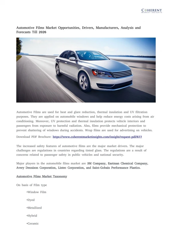
Download
1 / 4
0 likes | 9 Views
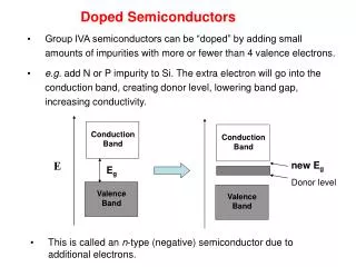
u00a0Dopingu00a0inu00a0theu00a0manufactureu00a0ofu00a0semiconductorsu00a0refersu00a0tou00a0theu00a0purposefulu00a0introductionu00a0of impuritiesu00a0intou00a0anu00a0inherentu00a0semiconductoru00a0withu00a0theu00a0goalu00a0ofu00a0modifyingu00a0itsu00a0structural,u00a0optical,u00a0and electricalu00a0properties

E N D
Search Your Style (https://mobilityforesights.com/) Your Cart 0 Your Name Your cart is empty Business Email Return to Shop (https://mobilityforesights.com/marketreports/) Country Phone Number +82 Company Name Your message By submitting this form, you are agreeing to the Terms of Use (https://mobilityforesights.com/termsconditions/) and Privacy Policy (https://mobilityforesights.com/privacypolicy/). DOWNLOAD SAMPLE 0 Continue Shopping (https://mobilityforesights.com/wpcontent/uploads/2022/10/Semiconductor30.png) Global Doped Films Market 2024-2030 Single User License : $ 4,000 Corporate User License : $ 6,000 Request Sample (https://mobilityforesights.com/contact-us/?report=35517) BUY NOW DESCRIPTION TABLE OF CONTENTS DOPED FILMS MARKET
INTRODUCTION Doping in the manufacture of semiconductors refers to the purposeful introduction of impurities into an inherent semiconductor with the goal of modifying its structural, optical, and electrical properties. An extrinsic semiconductor is the term used to describe the doped substance.A semiconductor’s capacity to conduct electricity can vary with the addition of a few dopant atoms. When a semiconductor is doped, the permissible energy levels are introduced into the crystal’s band gap, but very near the energy band that corresponds to the dopant type. In other words, electron acceptor impurities produce states close to the valence band, whereas electron donor impurities produce states close to the conduction band. DOPED FILMS MARKET SIZE AND FORECAST The Global doped films market accounted for $XX Billion in 2023 and is anticipated to reach $XX Billion by 2030, registering a CAGR of XX% from 2024 to 2030. DOPED FILMS MARKET DYNAMICS Firstprinciples calculations and experimental research combined to examine doping of ultra thin Si films. Considering doped Si films with two distinct doping concentrations, quantum confinementinduced bandgap widening has been examined. Dopant formation energy development that is thicknessdependent is also retrieved for thin films. The results clearly show that doping thinner films is more challenging and that dopant positioning near the surface is energetically more advantageous than core dopants. But compared to the surface dopant, the core dopant produces a larger density of states. Dopantinduced states above the conduction band edge and changes to the intrinsic film states can be seen when the carrier states in the doped Si film are projected onto those of a reference intrinsic film. Additionally, the ex situ phosphorusdoped ultrathin Sionoxide with a thickness of 4.5 nm by the beamline ion implantation technique was used to experimentally evaluate the ab initio predictions. The thickness of the Si coating on oxide has been established by highresolution
transmission electron microscopy. The effective dopant activation energy of the ionimplanted phosphorus dopant was determined by temperaturedependent electrical characterization on the transfer length method test structures to be 13.5 meV, which is consistent with our theoretical predictions for a similar film thickness. This paves the door to achieving the technology required for the next generation of Sibased electronic devices, which depend on ultrathin Si films. DOPED FILMS MARKET COMPANY PROFILES Cambrios Technologies Corporation Canatu Oy (https://canatu.com/carbonnanotube/canatucntproductplatforms/canatu transparentconductivefilms/) Dontech Inc DuPont de Nemours Inc (https://www.dupont.com/electronicmaterials/polyimide films.html/) Eastman Kodak Company Gunze Limited (https://www.gunze.co.jp/english/products/plasticfilms/index.html) Nitto Denko Corporation (https://www.nitto.com/in/en/products/optical/structure009/) OIKE & Co. Ltd TDK Corporation (https://product.tdk.com/en/techlibrary/developing/agstack/index.html) Toyobo Co. Ltd (https://www.toyobo global.com/seihin/film/package/list/productslist.html) DOPED FILMS MARKET REPORT WILL ANSWER FOLLOWING QUESTIONS 1. How many Doped Films are manufactured per annum globally? Who are the sub component suppliers in different regions? 2. Cost breakup of a Global Doped Films and key vendor selection criteria 3. Where is the Doped Films manufactured? What is the average margin per unit? 4. Market share of Global Doped Films market manufacturers and their upcoming products 5. Cost advantage for OEMs who manufacture Global Doped Films inhouse 6. key predictions for next 5 years in Global Doped Films market 7. Average B2B Doped Films market price in all segments 8. Latest trends in Doped Films market, by every market segment 9. The market size (both volume and value) of the Doped Films market in 20242030 and every year in between? 10. Production breakup of Doped Films market, by suppliers and their OEM relationship RELATED REPORTS
MARKET REPORTS CONSUMER RESEARCH INFORMATION ADVISORY SERVICES CONTACT INFORMATION 172/1, 2nd Floor, 5th Main, 9th Cross Rd, Opposite to Kairalee Nikethan Education Trust, Indira Nagar 1st Stage, Bengaluru, Karnataka 560038, INDIA +1 217 636 3356, +44 20 3289 9440 sales@mobilityforesights.com Working Hours: Mon Fri (9 AM 9 PM IST) Connect with us (https://www.facebook.com/mobilityforesights/) (https://twitter.com/mforesights) (https://www.linkedin.com/company/mobilityforesights privatelimited) (https://www.youtube.com/@mobilityforesights) © Copyright 20172023. Mobility Foresights. All Rights Reserved.