Doped Semiconductors
230 likes | 1.48k Views
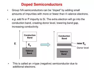
Conduction Band. Conduction Band. E. new E g . E g . Donor level. Valence Band. Valence Band. Doped Semiconductors. Group IVA semiconductors can be “doped” by adding small amounts of impurities with more or fewer than 4 valence electrons.

Doped Semiconductors
E N D
Presentation Transcript
Conduction Band Conduction Band E new Eg Eg Donor level Valence Band Valence Band Doped Semiconductors • Group IVA semiconductors can be “doped” by adding small amounts of impurities with more or fewer than 4 valence electrons. • e.g. add N or P impurity to Si. The extra electron will go into the conduction band, creating donor level, lowering band gap, increasing conductivity. • This is called an n-type (negative) semiconductor due to additional electrons.
Conduction Band E Eg Valence Band p-Type Semiconductors • Adding an impurity with fewer electrons e.g. add B or Al to Si, results in the formation of an acceptor level above the valence band, easily accessible to the valence band. This also lowers the band gap. Conduction Band Acceptor level new Eg Valence Band • This is called a p-type (positive) semiconductor as “holes” (positive charge carriers) are left behind in the valence band.
Figure 12.39 Crystal structures and band representations of doped semiconductors
Diodes • If p– and n–type semiconductors are joined together, a “p–n” junction is obtained. • If this is made part of a circuit, with the n-type end connected to a negative voltage, electrons will flow from donor groups across junction, holes will move other way, leads to flow of current. • If circuit is connected up the other way, donor electrons will be attracted to positive terminal – no flow of current. • Thus, a diode only allows current to flow in one direction.
p-n junction The p-n junction Figure 12.40 Forward bias Reverse bias
LEDs • When free electrons in a diode move into holes of p–type layer, the drop in energy from the conduction band to a lower orbital. This can result in the emission of light. • The band gap energy can by “tuned” by composition of semiconductor, as discussed earlier. The energy difference can be made to correspond to visible light (E = hc/l). This is called a Light Emitting Diode.
Resistance Temperature Resistance Temperature Resistance • Resistance is the opposition to the flow of current (units Ohm – W) Conductors Resistance increases with T, due to increasing atomic vibration hindering electron mobility Semiconductors Resistance decreases with T, as fraction of electrons able to overcome band gap increases
Resistance Temperature Superconductors • For certain substances, resistance drops to zero below a critical temperature, Tc • Under such conditions, current can flow completely unimpeded. • Potential uses of superconductors include power transmission (avoiding loss due to heating), and as strong magnets. • Meissner effect: Superconductors are perfect diamagnets, so strongly repel magnetic fields with less than the critical field strength (Hc). • So, to be superconducting, must be < Tc, and not in presence of magnet > Hc • Breakthrough in late 1980’s: ceramic superconductors with Tc > liquid nitrogen temperature (77 K).