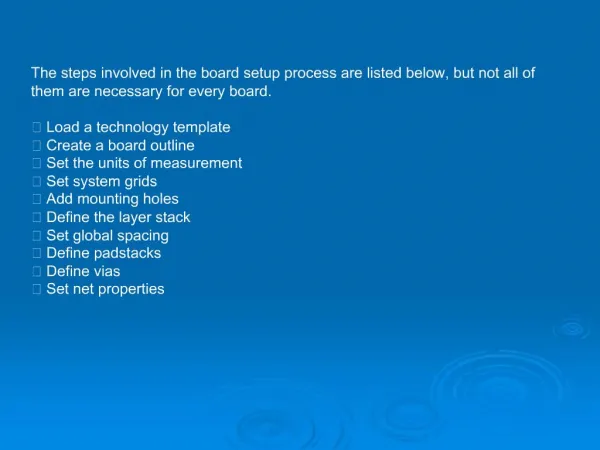
Step-by-Step PCB Layout Planning with OrCAD X Software
0 likes | 9 Views
Master the essentials of PCB layout planning with a step-by-step guide using OrCAD X software. Learn how to optimize schematic capture, component placement, and routing strategies for efficient designs. This guide helps you enhance signal integrity and manufacturability with practical tips. Discover key techniques and streamline your workflow with expert insights. Ideal for beginners and experienced designers using an OrCAD PCB designer platform.

Step-by-Step PCB Layout Planning with OrCAD X Software
E N D
Presentation Transcript
Introduction to PCB Layout Planning Effective PCB layout planning forms the backbone of any successful electronic design. It ensures optimized performance, reduced errors, and better manufacturability. Understanding how to structure a PCB layout systematically helps designers avoid costly mistakes later. A well-planned approach, combined with the right tools like an OrCAD PCB designer, allows for greater accuracy and efficiency throughout the development process.
Setting Clear Design Requirements Before starting any PCB layout, it's important to define clear electrical, mechanical, and functional requirements. Setting these upfront saves significant time during the layout stage. Focus on aspects like board dimensions, component specifications, and critical signal paths. With a structured checklist, designers can better align the layout with the intended performance standards without repetitive revisions.
Schematic Capture and Organization An organized schematic is the foundation of a smooth PCB layout process. Keeping the schematic neat, using consistent labeling, and grouping related components logically helps during the layout phase. Designers often rely on professional tools to maintain schematic clarity. Proper schematic capture also supports smoother netlist generation and error-free routing in later steps.
Creating the PCB Layout Outline Defining the physical board outline early provides a clear framework for component placement. Attention should be given to keep-out areas, mechanical holes, and height restrictions. At this stage, using tools with flexible outline management features makes a difference. To explore more detailed techniques, you can check this guide on how to use OrCAD X for PCB layout planning for step-by-step insights.
Strategic Component Placement Smart component placement is key to achieving optimal PCB performance. High-speed components should be positioned to minimize signal path lengths. Power devices must be placed to improve heat dissipation. An OrCAD PCB designer allows layout engineers to simulate and refine placements virtually, ensuring that critical components are placed logically to meet design objectives effectively.
Routing and Signal Integrity Focus Once placement is completed, attention turns to routing. Prioritize critical nets first and apply design rules for impedance control, especially for high-frequency signals. Keep traces as short and direct as possible to enhance signal integrity. Also, consider via minimization strategies during this stage. A careful routing strategy drastically improves the PCB’s overall performance and reliability.
Preparing for Fabrication and Final Review The final stage involves preparing manufacturing files such as Gerbers, BOMs, and assembly drawings. Always conduct a thorough design review to ensure every aspect meets the original requirements. Clear documentation and proper file generation guarantee a smoother transition from design to production, leading to high-quality PCB fabrication and assembly outcomes.