PCB Reverse Engineering And Its Methods
To know everything about the PCB Reverse Engineering And Its Methods visit: https://bit.ly/2BrxGQz

PCB Reverse Engineering And Its Methods
E N D
Presentation Transcript
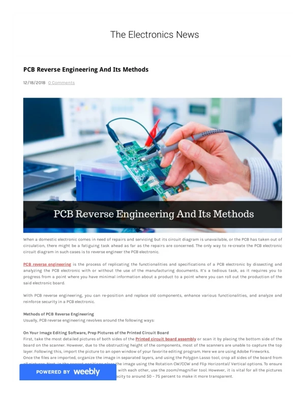
The Electronics News PCB Reverse Engineering And Its Methods 12/18/2018 0 Comments When a domestic electronic comes in need of repairs and servicing but its circuit diagram is unavailable, or the PCB has taken out of circulation, there might be a fatiguing task ahead as far as the repairs are concerned. The only way to re-create the PCB electronic circuit diagram in such cases is to reverse engineer the PCB electronic. PCB reverse engineering is the process of replicating the functionalities and specifications of a PCB electronic by dissecting and analyzing the PCB electronic with or without the use of the manufacturing documents. It’s a tedious task, as it requires you to progress from a point where you have minimal information about a product to a point where you can roll out the production of the said electronic board. With PCB reverse engineering, you can re-position and replace old components, enhance various functionalities, and analyze and reinforce security in a PCB electronic. Methods of PCB Reverse Engineering Usually, PCB reverse engineering revolves around the following ways: On Your Image Editing Software, Prep Pictures of the Printed Circuit Board First, take the most detailed pictures of both sides of the Printed circuit board assembly or scan it by placing the bottom side of the board on the scanner. However, due to the obstructing height of the components, most of the scanners are unable to capture the top layer. Following this, import the picture to an open window of your favorite editing program. Here we are using Adobe Fireworks. Once the files are imported, organize the image in separated layers, and using the Polygon Lasso tool, crop all sides of the board from all pictures. Next, in the correct positions place the image using the Rotation CW/CCW and Flip Horizontal/ Vertical options. To ensure that all the sides of the images properly aligned with each other, use the zoom/magnifier tool. However, it is vital for all the pictures to be correctly aligned. Reduce the top layer’s opacity to around 50 – 75 percent to make it more transparent. POWERED BY POWERED BY
Combine the Images There are copious ways to coalesce images, to have a range of options available for you to choose the one that works best for you, depending on your board color, illumination, and other optical factors. Screen Amalgam: Drag the bottom side up towards the component side to use screen amalgam. Then, to dim the copper layer, set the bar in the Brightness/Contrast filter to - 50. Next, highlight the copper layer and then choose blend mode on the Screen/Interpolation or Average (set to 80). Luminosity Blend: Drag the bottom side up towards the component side, and use the Levels filters to increase the contrast of the copper layer. Following, highlight the copper layer and select blend mode in Luminosity and set to 50. Brush and Threshold the Picture Drag the bottom side upwards toward the component side, and highlight the copper area by drawing a network of lines that connect the solder pads and holes using Brush. It is advisable to select colors that do not match with the solder mask. Later, extract only the solid color using the levels filter or threshold filter, and move the left pin across to the right. Ensuring this, adjust the Hue/saturation filter and select your preferred track color, rotating the Hue. Next, choose the blend in additive mode by highlighting the copper layer, and adjust the track’s intensity by setting the opacity to around 70. The last and final step is to record the values and replicate the benefits on CAD software. Hence, PCB engineering is a tedious task that requires not only expert technical knowledge but also a lot of strength of character. At PCC, we have a dedicated team of engineers with proficiency and understanding of PCB Reverse Engineering Process. Our engineering expert team follow IPC design specifications and will work on simple to the most complex PCB/PCA projects. Our PCB and PCA knowledge with extensive years of manufacturing experience has enabled us to provide optimum PCB Reverse Engineering Services. Like 0 Tweet 0 Comments Leave a Reply. POWERED BY POWERED BY
Name (required) Email (not published) Website Comments (required) Notify me of new comments to this post by email SUBMIT Categories All Cable And Wire Contract Manufacturers EMS PCB Reverse Enginering RSS Feed POWERED BY POWERED BY