Download
1 / 2
0 likes | 60 Views
The process of manufacturing semiconductors is highly complex, involving multiple stages of precision engineering and advanced materials science.

E N D
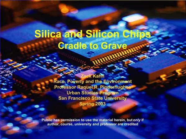
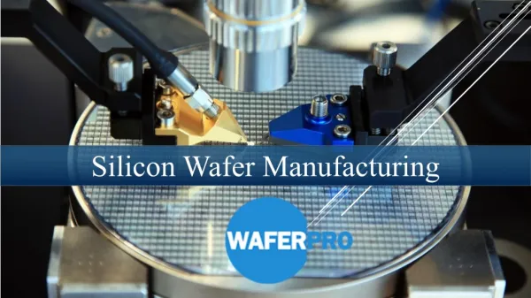
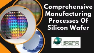
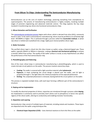
From Silicon To Chips: Understanding The Semiconductor Manufacturing Process Semiconductors are at the core of modern technology, powering everything from smartphones to supercomputers. The process of manufacturing semiconductors is highly complex, involving multiple stages of precision engineering and advanced materials science. This blog explores the key steps involved in transforming raw silicon into functional semiconductor chips. 1. Silicon Extraction and Purification The semiconductor production process begins with silicon, which is derived from silica (SiO₂), commonly found in sand. To be used in semiconductor manufacturing, silicon must be purified to an extremely high level—99.9999% or higher. This is achieved through a process called the Czochralski method, in which raw silicon is melted and crystallized into a large, highly pure monocrystalline silicon ingot. 2. Wafer Formation The purified silicon ingot is sliced into thin discs known as wafers using a diamond-tipped saw. These wafers, typically 200mm to 300mm in diameter, undergo chemical and mechanical polishing to achieve a smooth, defect-free surface. The quality of the wafer surface is crucial, as any imperfections can affect the performance of the final semiconductor chip. 3. Photolithography and Patterning One of the most critical steps in semiconductor manufacturing is photolithography, which is used to create intricate circuit patterns on the wafer. The process involves several key steps: • • Coating: The wafer is covered with a light-sensitive material called photoresist. Exposure: A mask containing the circuit design is placed over the wafer, and UV light is projected through it. The light alters the chemical properties of the exposed photoresist. Etching: The unwanted photoresist is removed, leaving behind the circuit pattern on the wafer. • This process is repeated multiple times, with each layer forming a different part of the semiconductor’s structure. 4. Doping and Ion Implantation To modify the electrical properties of silicon, impurities are introduced through a process called doping. Ion implantation is commonly used to precisely insert atoms such as phosphorus or boron into specific regions of the silicon wafer, altering its conductivity and enabling transistor functionality. 5. Deposition and Layering Semiconductor chips consist of multiple layers of materials, including metals and insulators. These layers are deposited onto the wafer using techniques like: • Chemical Vapor Deposition (CVD)– Uses chemical reactions to form thin films on the wafer.
• Physical Vapor Deposition (PVD)– Deposits materials via high-energy plasma. Each layer plays a role in forming transistors, capacitors, and interconnects essential for the chip’s operation. 6. Etching and Planarization After deposition, unwanted material is removed using etching techniques. Wet etching (chemical-based) and dry etching (plasma-based) are used depending on the required precision. Chemical Mechanical Planarization (CMP) is then applied to smooth the wafer surface, ensuring uniformity across layers. 7. Testing and Packaging Once fabrication is complete, the wafers undergo electrical testing to identify defective chips. Functional chips are then cut from the wafer and enclosed in protective packaging. The packaging process involves attaching the chip to a circuit board, adding wiring for connectivity, and sealing it to protect against environmental damage. The semiconductor manufacturing process is a highly sophisticated and precise operation, requiring advanced materials, equipment, and engineering techniques. As technology continues to evolve, manufacturers are constantly pushing the boundaries of miniaturization and efficiency, enabling the development of smaller, faster, and more powerful semiconductor chips.