Download
1 / 11
580 likes | 2.65k Views
Application of photodiodes. A brief overview. Diode devices. Check valve behavior Diffusion at the PN junction of P into N and N into P causes a depleted non-conductive region Depletion is enhanced by reverse bias Depletion is broken down by forward bias When forward biased

E N D
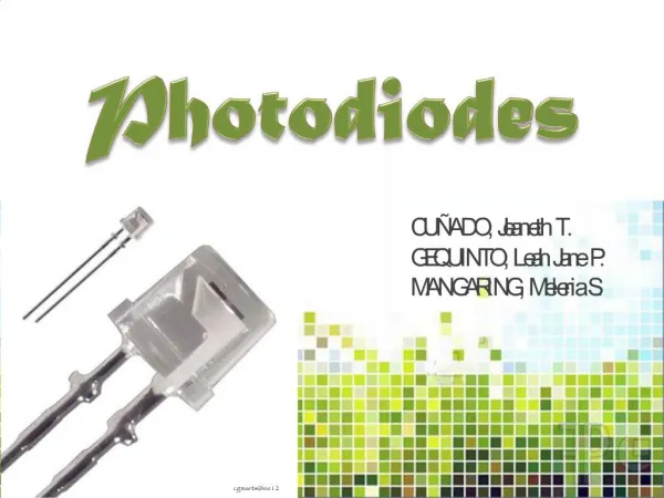
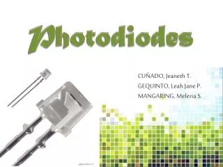
Application of photodiodes A brief overview BAE 5413
Diode devices • Check valve behavior • Diffusion at the PN junction of P into N and N into P causes a depleted non-conductive region • Depletion is enhanced by reverse bias • Depletion is broken down by forward bias • When forward biased • High current flow junction voltage • When reverse biased • Very low current flow unless above peak inverse voltage (PIV) (damaging to rectifying diodes, OK for zeners) BAE 5413
Quantum devices • Absorption of a photon of sufficient energy elevates an electron into the conduction band and leaves a hole in the valence band. • Conductivity of semi-conductor is increased. • Current flow in the semi-conductor is induced. BAE 5413
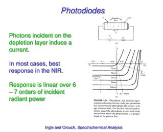
Photodiode structure Absorbtion in the depletion layer causses current to flow across the photodiode and if the diode is reverse biased considerable current flow will be induced BAE 5413
Photodiode fundamentals • Based on PN or PIN junction diode • photon absorption in the depletion region induces current flow • Depletion layer must be exposed optically to source light and thick enough to interact with the light • Spectral sensitivity BAE 5413
Photodiode characteristics • Circuit model • I0 Dark current (thermal) • Ip Photon flux related current • Noise characterization • Shot noise (signal current related) • q = 1.602 x 10⁻¹⁹ coulombs • I = bias (or signal) current (A) • is = noise current (A rms) • Johnson noise (Temperature related) • k = Boltzman’s constant = 1.38 x 10⁻²³ J/K • T = temperature (°K) • B = noise bandwidth (Hz) • R = feedback resistor (W) • eOUT = noise voltage (Vrms) BAE 5413
Trans-impedance amplifier function • Current to voltage converter (amplifier) • Does not bias the photodiode with a voltage as current flows from the photodiode (V1 = 0) • Circuit analysis • Note: current to voltage conversion BAE 5413
Diode operating modes • Photovoltaic mode • Photodiode has no bias voltage • Lower noise • Lower bandwidth • Logarithmic output with light intensity • Photoconductive mode • Higher bandwidth • Higher noise • Linear output with light intensity BAE 5413
For the photovoltaic mode • I = thermal component + photon flux related current • where I = photodiode current V = photodiode voltage I0 = reverse saturation current of diode e = electron charge k = Boltzman's constant T = temperature (K) n = frequency of light h = Plank’s constant P = optical power h = probability that hv will elevate an electron across the band gap BAE 5413
Circuit Optimization • Burr-Brown recommendations (TI) • Photodiode capacitance should be as low as possible. • Photodiode active area should be as small as possible so that CJ is small and RJ is high. • Photodiode shunt resistance (RJ ) should be as high as possible. • For highest sensitivity use the photodiode in a “photovoltaic mode”. • Use as large a feedback resistor as possible (consistent with bandwidth requirements) to minimize noise. • Shield the photodetector circuit in a metal housing. • A small capacitor across Rf is frequently required to suppress oscillation or gain peaking. • A low bias current op amp is needed to achieve highest sensitivity BAE 5413