Download
1 / 22
290 likes | 1.1k Views
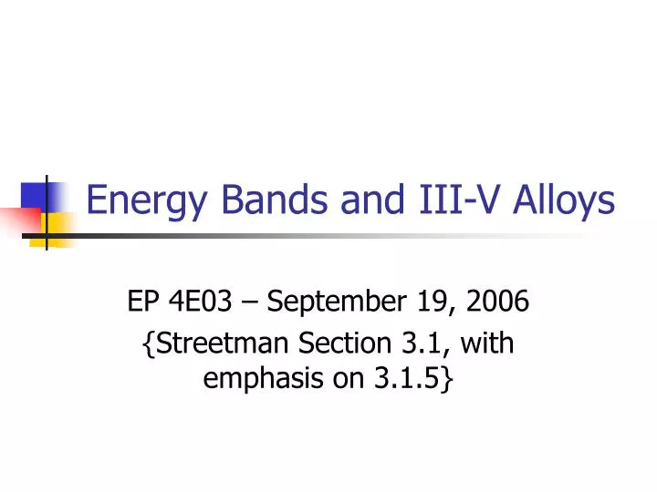
Energy Bands and III-V Alloys. EP 4E03 – September 19, 2006 {Streetman Section 3.1, with emphasis on 3.1.5}. Goals. Review, in a qualitative manner, the underlying principles of energy bands in solids; Discuss the importance of III-V materials: Introduction to various alloys,

E N D
Energy Bands and III-V Alloys EP 4E03 – September 19, 2006 {Streetman Section 3.1, with emphasis on 3.1.5}
Goals • Review, in a qualitative manner, the underlying principles of energy bands in solids; • Discuss the importance of III-V materials: • Introduction to various alloys, • Main applications, • Design considerations. Note:This presentation does not strictly follow Streetman’s treatment, but instead introduces the topics in a different manner. Moreover, a wider coverage of the important III-V materials is provided.
In the solid, the separation between the constituting atoms is comparable to the atomic size, so the properties of the individual atoms are altered by the presence of neighbouring atoms. Review of Energy Bands (1) In crystalline solids, the atoms are “assembled” in a periodical arrangement, in such a way as to minimize the energy of the system… Example: NaCl crystal (ionic bound) Kasap, S.O., Principles of electrical engineering materials and devices, McGraw-Hill, 1997
Since the solid is made of a very large number of atoms (N), these bands are actually constituted by N levels of energies (almost a continuum!). The position of upper and lower extreme of each band is however independent of N (depends only on the materials). Review of Energy Bands (2) Holden A., The nature of solids, Dover Publications, 1965 The permitted energies that an electron can occupy in the isolated atoms are split into energy bands as the atoms get closer to each other. This can also be visualized in terms of an overlap of the electron wave functions (Streetman section 3.1.2). Outer shell
a + b e.g. a 1-D crystal could for instance be represented in the following manner: Uo a Adapted from: R. Eisberg, R. Resnick, Quantum physics of atoms, molecules, solids, nuclei, and particles (2nd ed.), Wiley, 1985 b a + b x = 0 Review of Energy Bands (3) Mathematically, it means solving the time-independent Schrödinger’s equation: where U(r) is the periodic effective potential energy that describes the arrangement of atoms in the crystal.
Actual band diagram For device description a much more simple and practical representation is typically used: Eg ~ 1.4 eV Ec Eg Ev Cohen M.L., Chelikowski, J.R., Electronic Structure and Optical Properties of semiconductors, Springer, 1989 Review of Energy Bands (4) The solution to the equation is usually given in the form of a “band diagram” E vs k. Yu, P.Y., Cardona, M., Fundamentals of semiconductors, Springer, 2005 e.g.GaAs crystal
Review of Energy Bands (5) Direct band gap semiconductors (e.g. GaAs, InP, InAs, GaSb) The minimum of the conduction band occurs at the same k value as the valence band maximum. Eg ~ 1.4 eV Cohen M.L., Chelikowski, J.R., Electronic Structure and Optical Properties of semiconductors, Springer, 1989
Review of Energy Bands (6) Indirect band gap semiconductors (e.g. Si, Ge, AlAs, GaP, AlSb) The minimum of the conduction band does not occur at the same k value as the valence band maximum. An electron promoted to the conduction band requires a change of its momentum to make the transition to the valence band (typ. occurs via lattice vibrations). Eg ~ 2.3 eV Cohen M.L., Chelikowski, J.R., Electronic Structure and Optical Properties of semiconductors, Springer, 1989
III-V Materials Binary Compounds III IV V • Arsenides: GaAs, AlAs, InAs • Phosphides: GaP, AlP, InP • Antimonides: GaSb, AlSb, InSb • Nitrides: GaN, AlN, InN Tu, K-N, Mayer, J.W, Feldman, L.C., Electronic thin film science for electrical engineers and materials scientists, McMillan, 1992
Why III-V’s for devices? • Very low effective mass compared to Si (e.g. m*nl,Si = 0.98mo, m*n,GaAs = 0.067mo, m*n,InSb = 0.014mo): • This translates into very high electron mobilities for high-speed electronic applications. • A wide variety of these materials have a direct band gap: • Photon emission is most efficient during recombination processes, so very suitable for light sources (lasers, LED’s), but also detectors. • Possibility to create alloys consisting of the different elements: • The properties of the device (e.g. emission wavelength of a light source) can be tailored to suit the needs (“band gap engineering”).
1 Ternary III-V Alloys (1) The group III lattice sites are occupied by a fraction x of atoms III1 and a fraction (1-x) of atoms III2. Arsenides: e.g. InGaAs (used in the active regions of high-speed electronic devices, IR lasers, and long-wavelength quantum cascade lasers) Phosphides: e.g. InGaP (GaAs-based quantum well devices such as red diode lasers) Antimonides: e.g. AlGaSb (employed in high-speed electronic and infrared optoelectronic devices) Nitrides: e.g. InGaN (key constituent in the active regions of blue diode lasers and LED’s)
2 Ternary III-V Alloys (2) The group V lattice sites are occupied by a fraction y of atoms V1 and a fraction (1-y) of atoms V2. Arsenides Antimonides: e.g. InAsSb (smallest band gap of all III-V’s, very important material for mid-infrared optoelectronic devices) Arsenides Phosphides: e.g. GaAsP (often used for red LED’s) Phosphides Antimonides: e.g. GaPSb
GaxIn1-xP GaxIn1-xAs Ternary III-V Alloys (4) Band Gap Engineering: Arsenides, Phosphides, Antimonides http://www.rpi.edu/~schubert/Light-Emitting-Diodes-dot-org/chap07/F07-06-R.jpg
Ternary III-V Alloys (3) Band Gap Engineering: Nitrides l 207 nm 248 nm http://www.onr.navy.mil/sci_tech/31/312/ncsr/materials/gan.asp 310 nm 413 nm 620 nm 1.24 mm
However: • More elements → more fabrication issues!!! (e.g. composition control requires tedious calibration growths) • Range of stable compositions is limited due to the fact that in thermal equilibrium the components of the alloy often tend to segregate into inhomogeneous mixture of binaries and ternaries… Quaternary III-V Alloys (1) Why? Provide even greater flexibility in device design…
Quaternary III-V Alloys (2) The case of GaxIn1-xAsyP1-y Wide variety of compositions (hence various emission wavelengths) are lattice matched to either GaAs or InP… Panish, M.B., Temkin, H., Gas source Molecular Beam Epitaxy, Springer, 1993
The misfit is defined as: as : lattice constant of the substrate material af : lattice constant of the film material Design Considerations Most practical devices consists in heterostructures, i.e. layered thin film structures made of dissimilar materials deposited on top of each other (e.g. quantum well). Based on the device requirements, the designer will select the proper alloy, while keeping in mind that typical substrates consist in binary compound (such as GaAs, InP, InP, GaSb) in order to minimize the effects of lattice mismatch.
Lattice-matched structure By definition, f = 0, i.e. both the substrate material and the film material have the same lattice constant. A misfit |f| < 5 × 10⁻⁴ is generally considered very good, and for practical purposes is assumed lattice-matched (e.g. AlGaAs/GaAs structures) Ohring, M., The Materials Science of Thin Films, Academic Press, 1992
Strained Structures f ≠ 0 (i.e. as ≠ af) f < 0 : compressive strain f > 0 : tensile strain For relatively thin film thicknesses, cubic crystals will distort (strain develops within the layer) to achieve the same in-plane lattice constant. Such a layer is referred to as pseudomorphic. Ohring, M., The Materials Science of Thin Films, Academic Press, 1992
Burgers vector: atomic displacement needed to generate the dislocation In the process, defects known as misfit dislocations form at the interface… Tu, K-N, Mayer, J.W, Feldman, L.C., Electronic thin film science for electrical engineers and materials scientists, McMillan, 1992 Relaxed Structure Beyond a certain critical thickness hc, it is energetically more favourable for the film to “relax”, i.e. achieve a state where its lattice constant tends towards its unstrained value.
Critical Thickness (1) hc is obtained by minimizing Etot with respect to the strain. This results in a transcendent equation: where n is the Poisson’s ratio of the film material.
Mayer, J.W, Lau, S.S., Electronic Materials Science: For integrated circuits in Si and GaAs, McMillan, 1990 Critical Thickness (2)