Download
1 / 2
0 likes | 9 Views
The advanced packaging lithography system market is poised for growth, driven by the increasing demand for high-performance semiconductors in AI, 5G, and IoT applications. Key trends include the shift towards heterogeneous integration, miniaturization of electronic components, and the development of advanced packaging techniques like fan-out wafer-level packaging (FOWLP). Asia-Pacific is expected to lead the market due to its strong semiconductor manufacturing base, while ongoing innovations aim to enhance precision and throughput in packaging processes.

E N D
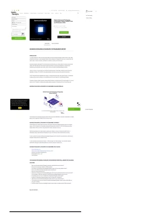
+1 217 636 3356 +44 20 3289 9440 sales@mobilityforesights.com Your Cart 0 Company Market Reports Consumer Research Advisory Services Exports - Imports Careers Contact Us Blog Your cart is empty Your Name Return to Shop Business Email Global Advanced Packaging Lithography System Market Size and Forecasts 2030 Country Phone Number +82 Company Name Single User License : $ 4,000 Your message Corporate User License : $ 6,000 By submitting this form, you are agreeing to the Terms of Use and Privacy Policy. Request Sample I'm not a robot reCAPTCHA Privacy - Terms BUY NOW DOWNLOAD SAMPLE DESCRIPTION TABLE OF CONTENTS ADVANCED PACKAGING LITHOGRAPHY SYSTEM MARKET REPORT INTRODUCTION To produce features for 2.5D and 3D advanced packages, Advanced packaging lithography system employs a step, settle, and illuminate technique. To build multiplayer features, these operations are repeated from die to die on a single wafer, from wafer to wafer on the same machine, and finally from machine to machine on the factory floor. Advanced packages’ complicated 2.5D and 3D structures must be built up over a large number of exposures using several reticles, which might slow down the process. By making dies larger, the industry has attempted to counteract poorer throughput by processing fewer die per wafer, which cuts down on Advanced packaging lithography system Larger die, however, call for a higher level of surface positioning precision. Theta stage with high accuracy and dynamic capabilities, innovative Z Tip Tilt (ZTT), and excellent alignment and accuracy between the die and the die surface. The ZTT stage has focusing capabilities that enable it to dynamically keep the wafer in the proper Z position. By addressing the alignment and accuracy problems, these capabilities permit the use of larger die in sophisticated packaging. Increasing the speed of wafer movement in between flash illuminations is another technique to boost throughput. For moving masses in the XY direction, air bearing motion stage typically accelerates at 1-2g with a jerk time of a few milliseconds. ADVANCED PACKAGING LITHOGRAPHY SYSTEM MARKET SIZE AND FORECAST We use cookies to understand site usage and improve content and offerings on our site. To learn more, refer to our Privacy Policy. By continuing to use this site, or closing this box, 0 Learn more you consent to our use of cookies. Got it! Send message Continue Shopping The Global Advanced packaging lithography system market accounted for $XX Billion in 2023 and is anticipated to reach $XX Billion by 2030, registering a CAGR of XX% from 2024 to 2030. ADVANCED PACKAGING LITHOGRAPHY SYSTEM MARKET DYNAMICS The FPA-5520iV LF2 Option for back-end process semiconductor Advanced packaging lithography system i-line stepper1 systems, which contributes to 3D advanced packaging technologies with a resolution of 0.8 m (micrometer2) and a wide exposure field of 100 mm x 100 mm, was just launched in Japan, according to canon Inc. Higher-density packing in back-end processes is gaining more attention in the area of improving the performance of semiconductor chips, coupled with the downsizing of circuits in the front-end process of semiconductor production. In order to achieve fine rewiring for Advanced packaging lithography systems that deliver high performance, semiconductor lithography methods have been adopted recently. In order to increase semiconductor performance, “2.5D technology3” and “3D technology4”, both of which incorporate semiconductor chips with exceptionally high die-to-die connection densities, are being used. ADVANCED PACKAGING LITHOGRAPHY SYSTEM MARKET KEY PLAYERS Amkor Technology, Inc. Taiwan Semiconductor Manufacturing Company, Limited Advanced Semiconductor Engineering Inc. Samsung Electronics Co., Ltd Intel Corporation THIS ADVANCED PACKAGING LITHOGRAPHY SYSTEM MARKET REPORT WILL ANSWER THE FOLLOWING QUESTIONS 1. How many Advanced packaging lithography systems are manufactured per annum globally? 2. Who are the sub-component suppliers in different regions? 3. Cost breakup of a Global Advanced packaging lithography system and key vendor selection criteria? 4. Where is the Advanced packaging lithography system manufactured? 5. What is the average margin per unit? 6. Market share of Global Advanced packaging lithography system market manufacturers and their upcoming products? 7. Cost advantage for OEMs who manufacture Global Advanced packaging lithography system in-house. 8. key predictions for next 5 years in Global Advanced packaging lithography system market? 9. Average B-2-B Advanced packaging lithography system market price in all segments? 10. Latest trends in Advanced packaging lithography system market, by every market segment? 11. The market size (both volume and value) of the Advanced packaging lithography system market in 2024-2030 and every year in between? 12. Production breakup of Advanced packaging lithography system market, by suppliers and their OEM relationship? RELATED REPORTS
MARKET REPORTS CONSUMER RESEARCH INFORMATION ADVISORY SERVICES CONTACT INFORMATION 172/1, 2nd Floor, 5th Main, 9th Cross Rd, Opposite to Kairalee Nikethan Education Trust, Indira Nagar 1st Stage, Bengaluru, Karnataka 560038, INDIA +1 217 636 3356, +44 20 3289 9440 sales@mobilityforesights.com Working Hours: Mon - Fri (9 AM - 9 PM IST) Connect with us © Copyright 2017-2023. Mobility Foresights. All Rights Reserved.