Download
1 / 7
210 likes | 1.57k Views
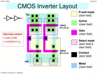
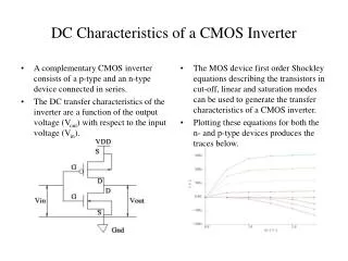
A complementary CMOS inverter consists of a p-type and an n-type device connected in series. The DC transfer characteristics of the inverter are a function of the output voltage (V out ) with respect to the input voltage (V in ).

E N D
A complementary CMOS inverter consists of a p-type and an n-type device connected in series. The DC transfer characteristics of the inverter are a function of the output voltage (Vout) with respect to the input voltage (Vin). The MOS device first order Shockley equations describing the transistors in cut-off, linear and saturation modes can be used to generate the transfer characteristics of a CMOS inverter. Plotting these equations for both the n- and p-type devices produces the traces below. DC Characteristics of a CMOS Inverter
The DC transfer characteristic curve is determined by plotting the common points of Vgs intersection after taking the absolute value of the p-device IV curves, reflecting them about the x-axis and superimposing them on the n-device IV curves. We basically solve for Vin(n-type) = Vin(p-type) and Ids(n-type)=Ids(p-type) The desired switching point must be designed to be 50 % of magnitude of the supply voltage i.e. VDD/2. Analysis of the superimposed n-type and p-type IV curves results in five regions in which the inverter operates. Region A occurs when 0 leqVin leq Vt(n-type). The n-device is in cut-off (Idsn =0). p-device is in linear region, Idsn = 0 therefore -Idsp = 0 Vdsp = Vout – VDD, but Vdsp =0 leading to an output of Vout = VDD. Region B occurs when the condition Vtn leq Vin le VDD/2 is met. Here p-device is in its non-saturated region Vds neq 0. n-device is in saturation Saturation current Idsn is obtained by setting Vgs = Vin resulting in the equation: DC Characteristics of a CMOS Inveter
In region B Idsp is governed by voltages Vgs and Vds described by: Region C has that both n- and p-devices are in saturation. Saturation currents for the two devices are: Region D is defined by the inequality p-device is in saturation while n-device is in its non-saturation region. Equating the drain currents allows us to solve for Vout. (See supplemental notes for algebraic manipulations). CMOS Inverter Transfer Characteristics
In Region E the input condition satisfies: The p-type device is in cut-off: Idsp=0 The n-type device is in linear mode Vgsp = Vin –VDD and this is a more positive value compared to Vtp. Vout = 0 nMOS & pMOS Operating points CMOS Inverter Static Charateristics Vout =Vin-Vtp A VDD B Vout =Vin-Vtn Both in sat C nMOS in sat Output Voltage pMOS in sat D E 0 VDD/2 VDD+Vtp VDD Vtp Vtn