Download
1 / 19
190 likes | 495 Views
EE130 Lecture 5, Slide 2. Intrinsic Fermi Level, Ei. To find EF for an intrinsic semiconductor, use the fact that n = p:. EE130 Lecture 5, Slide 3. n(ni, Ei) and p(ni, Ei). In an intrinsic semiconductor, n = p = ni and EF = Ei :. EE130 Lecture 5, Slide 4. Example: Energy-band diagram. Question: Where is EF for n = 1017 cm-3 ?.

E N D
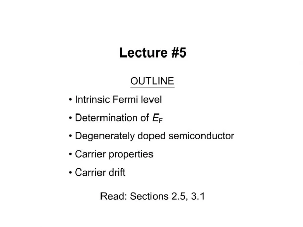
1. Lecture #5 OUTLINE
Intrinsic Fermi level
Determination of EF
Degenerately doped semiconductor
Carrier properties
Carrier drift
Read: Sections 2.5, 3.1
2. EE130 Lecture 5, Slide 2 Intrinsic Fermi Level, Ei To find EF for an intrinsic semiconductor, use the fact that n = p:
3. EE130 Lecture 5, Slide 3 n(ni, Ei) and p(ni, Ei) In an intrinsic semiconductor, n = p = ni and EF = Ei :
4. EE130 Lecture 5, Slide 4 Example: Energy-band diagram Question: Where is EF for n = 1017 cm-3 ?
5. EE130 Lecture 5, Slide 5 Dopant Ionization Consider a phosphorus-doped Si sample at 300K with
ND = 1017 cm-3. What fraction of the donors are not ionized?
Answer: Suppose all of the donor atoms are ionized.
Then
Probability of non-ionization ?
6. EE130 Lecture 5, Slide 6 Nondegenerately Doped Semiconductor Recall that the expressions for n and p were derived using the Boltzmann approximation, i.e. we assumed
The semiconductor is said to be nondegenerately doped in this case.
7. EE130 Lecture 5, Slide 7 Degenerately Doped Semiconductor If a semiconductor is very heavily doped, the Boltzmann approximation is not valid.
In Si at T=300K: Ec-EF < 3kT if ND > 1.6x1018 cm-3
EF-Ev < 3kT if NA > 9.1x1017 cm-3
The semiconductor is said to be degenerately doped in this case.
Terminology:
�n+� ? degenerately n-type doped. EF ? Ec
�p+� ? degenerately p-type doped. EF ? Ev
8. EE130 Lecture 5, Slide 8 Band Gap Narrowing If the dopant concentration is a significant fraction of the silicon atomic density, the energy-band structure is perturbed ? the band gap is reduced by DEG :
9. EE130 Lecture 5, Slide 9 Mobile Charge Carriers in Semiconductors Three primary types of carrier action occur inside a semiconductor:
Drift: charged particle motion under the influence of an electric field.
Diffusion: particle motion due to concentration gradient or temperature gradient.
Recombination-generation (R-G)
10. EE130 Lecture 5, Slide 10 Electrons as Moving Particles
11. EE130 Lecture 5, Slide 11 Carrier Effective Mass In an electric field, E, an electron or a hole accelerates:
Electron and hole conductivity effective masses:
12. EE130 Lecture 5, Slide 12 Thermal Velocity
13. EE130 Lecture 5, Slide 13 Carrier Scattering Mobile electrons and atoms in the Si lattice are always in random thermal motion.
Electrons make frequent collisions with the vibrating atoms
�lattice scattering� or �phonon scattering�
increases with increasing temperature
Average velocity of thermal motion for electrons: ~107 cm/s @ 300K
Other scattering mechanisms:
deflection by ionized impurity atoms
deflection due to Coulombic force between carriers
�carrier-carrier scattering�
only significant at high carrier concentrations
The net current in any direction is zero, if no electric field is applied.
14. EE130 Lecture 5, Slide 14 Carrier Drift When an electric field (e.g. due to an externally applied voltage) is applied to a semiconductor, mobile charge-carriers will be accelerated by the electrostatic force. This force superimposes on the random motion of electrons:
15. EE130 Lecture 5, Slide 15 Electron Momentum
16. EE130 Lecture 5, Slide 16 Carrier Mobility
17. EE130 Lecture 5, Slide 17 Electron and Hole Mobilities
18. EE130 Lecture 5, Slide 18 Example: Drift Velocity Calculation
19. EE130 Lecture 5, Slide 19 Mean Free Path Average distance traveled between collisions
20. EE130 Lecture 5, Slide 20 Summary The intrinsic Fermi level, Ei, is located near midgap
Carrier concentrations can be expressed as functions of Ei and intrinsic carrier concentration, ni :
In a degenerately doped semiconductor, EF is located very near to the band edge
Electrons and holes can be considered as quasi-classical particles with effective mass m*
In the presence of an electric field e, carriers move with average drift velocity , where m is the carrier mobility
![[lecture#5]](https://cdn0.slideserve.com/109460/slide1-dt.jpg)