
Lithography Materials Market
E N D
Presentation Transcript
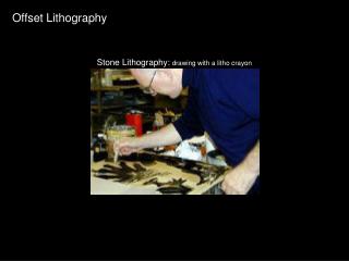
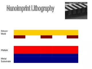
+1 217 636 3356 +44 20 3289 9440 sales@mobilityforesights.com Your Cart 0 Company Market Reports Consumer Research Advisory Services Exports - Imports Careers Contact Us Blog Your cart is empty Your Name Return to Shop Business Email Global Lithography Materials Market Size and Forecasts 2030 Country Phone Number +1 Company Name Single User License : $ 4,000 Your message Corporate User License : $ 6,000 By submitting this form, you are agreeing to Request Sample the Terms of Use and Privacy Policy. I'm not a robot reCAPTCHA Privacy - Terms BUY NOW DOWNLOAD SAMPLE DESCRIPTION TABLE OF CONTENTS LITHOGRAPHY MATERIALS MARKET INTRODUCTION Lithography is a process used to transfer patterns to materials for a variety of uses. It is used in the production of items such as integrated circuits, printed circuit boards, and other electronic components. The process involves the use of a light- sensitive material, called a photoresist, which is often a polymer. A photomask, which contains the pattern to be transferred, is placed on top of the photoresist. Ultraviolet light is then used to expose the photoresist, causing the exposed region to harden. The unexposed regions are then dissolved away with a chemical solution, leaving behind the pattern from the photomask. Lithography materials come in a variety of forms, including negative-tone and positive-tone photoresists. Negative-tone photoresists are developed by exposing the photoresist to UV light and then applying a developer. The exposed regions become insoluble and are removed with a developer, leaving behind the desired pattern. Positive-tone photoresists are developed by exposing the photoresist to UV light and then applying an etchant. The exposed regions become soluble and are removed with an etchant, leaving behind the desired pattern. In addition to photoresists, lithography materials also include resists such as dry-film resists, liquid resists, and abrasive resists. Dry-film resists are used in the production of printed circuit boards and are applied in liquid form. Liquid resists are applied by spraying and are used to create more intricate patterns. Abrasive resists are used to create patterns on metal surfaces. Lithography materials are essential in the manufacturing process of many products. They are used to create the intricate patterns needed for the production of items such as integrated circuits and printed circuit boards. As technology advances, 0 lithography materials will continue to be used in the production of a variety of products. LITHOGRAPHY MATERIALS MARKET SIZE AND FORECAST Continue Shopping The Global lithography materials market accounted for $XX Billion in 2023 and is anticipated to reach $XX Billion by 2030, registering a CAGR of XX% from 2024 to 2030. LITHOGRAPHY MATERIALS MARKET NEW LAUNCH The Japanese company Canon, which is best known for its printers and cameras, has introduced a vital tool that it claims will aid in the production of the most cutting-edge semiconductors available. Canon is taking on the Dutch company ASML, which is the market leader in extreme ultraviolet (EUV) lithography machines, with their newest “nanoimprint lithography” system.
The most cutting-edge chips, like those seen in the newest Apple iPhones made by Taiwan’s TSMC, cannot be made without ASML’s tools. The most cutting-edge chipmakers are using ASML’s EUV technology more and more since it is essential to producing semiconductors at 5 nanometers and smaller. The size of the features on a chip is indicated by the nanometer figure. More features can fit into a chip with a smaller figure, which boosts the semiconductor’s power. +1 LITHOGRAPHY MATERIALS MARKET RECENT DEVELOPMENTS A new chip tool from Applied Materials reduces lithography process costs. One of the major manufacturers of tools for the production of chips, Applied Materials Inc., located in Silicon Valley, announced on Tuesday that it has begun offering a new By submitting this form, you are agreeing to tool that can reduce the cost of a lithography process. the Terms of Use and Privacy Policy. The shiny spherical discs used to make chips called wafers are printed with a design using lithography and light. Each wafer may go through this process thousands of times. The wafer is put through a laborious process of material deposit, measurement to ensure appropriate printing of the pattern, etching out material to build transistors and other objects, and cleaning off the wafer to begin the process again. Additional techniques are required to match the demands as the patterns get smaller and smaller, eventually nearing the physical limit of what light can print. This is particularly true with the most recent lithography gear from the Dutch tool manufacturer ASML, which uses light with a wavelength known as extreme ultraviolet, or EUV. Repetition of a pattern twice is one of the tricks. The new instrument from Applied Materials, the Centura Sculpta, is used to sculpt the final pattern by shining a light on it just once for the initial pattern. THIS LITHOGRAPHY MATERIALS MARKET REPORT WILL ANSWER FOLLOWING QUESTIONS 1. How many lithography materials are manufactured per annum globally? Who are the sub-component suppliers in different regions? 2. Cost breakup of a Global lithography materials and key vendor selection criteria 3. Where are the lithography materials manufactured? What is the average margin per unit? 4. Market share of Global lithography materials market manufacturers and their upcoming products 5. Cost advantage for OEMs who manufacture Global lithography materials in-house 6. key predictions for next 5 years in Global lithography materials market 7. Average B-2-B lithography materials market price in all segments 8. Latest trends in lithography materials market, by every market segment 9. The market size (both volume and value) of the lithography materials market in 2024-2030 and every year in between? 10. Production breakup of lithography materials market, by suppliers and their OEM relationship RELATED REPORTS Global LED Strip Lights Market Size and Forecasts 2030 Europe Chemical Sensor Market 2022-2027 India Chemical Sensor Market 2022-2027 Global Silicon Nanochips Market 2024- 2030 $4,000 $4,000 Multi User Multi User $4,000 $4,000 Multi User Multi User License - License - MARKET REPORTS CONSUMER RESEARCH INFORMATION ADVISORY SERVICES CONTACT INFORMATION 172/1, 2nd Floor, 5th Main, 9th Cross Automotive and Transportation About Us Focus Group Study Transaction Advisory Rd, Opposite to Kairalee Nikethan Semiconductor Our Clientele Education Trust, Indira Nagar 1st Stage, Ethnographic Market Positioning Agriculture and Construction Our People Bengaluru, Karnataka 560038, INDIA Research Assessment Equipment Blog Brand Awareness Custom Automotive Aerospace and Defense +1 217 636 3356, +44 20 3289 9440 Contact us Study Market Research Marine and Rail Terms & Conditions sales@mobilityforesights.com Consumer Satisfaction Strategic Advisory Logistics and Packaging Privacy Policy Survey Competitive Working Hours: Mon - Fri (9 AM - 9 PM Medical Devices ESOMAR Guidelines Consumer Expectation Intelligence IST) Chemical and Materials Compliant & Loyalty Assessment Electrical Machinery Connect with us ICT Energy, Power and Robotics New Technologies © Copyright 2017-2023. Mobility Foresights. All Rights Reserved.