Download
1 / 20

E N D
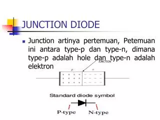
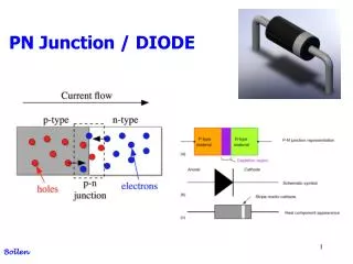
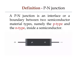
Definition - P-N junction A P-N junction is an interface or a boundary between two semiconductor material types, namely the p-type and the n-type, inside a semiconductor.
Formation of P-N Junction • If we use different semiconductor materials to make a P-N junction, there will be a grain boundary that would inhibit the movement of electrons from one side to the other by scattering the electrons and holes and thus, we use the process of doping.
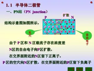
Formation of P-N Junction (process of doping ) • Let us consider a thin p-type silicon semiconductor sheet. If we add a small amount of pentavalent impurity to this, a part of the p-type Si will get converted to n-type silicon. • This sheet will now contain both the p-type region and the n-type region and a junction between these two regions.
Formation of P-N Junction • The processes that follow after forming a P-N junction are of two types – diffusion and drift. There is a difference in the concentration of holes and electrons at the two sides of a junction. • The holes from the p-side diffuse to the n-side, and the electrons from the n-side diffuse to the p-side. These give rise to a diffusion current across the junction.
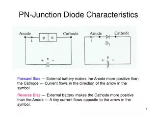
Conditions of P-N Junction Diode • Zero bias: No external voltage is applied to the P-N junction diode. • Forward bias: The positive terminal of the voltage potential is connected to the p-type while the negative terminal is connected to the n-type. • Reverse bias: The negative terminal of the voltage potential is connected to the p-type and the positive is connected to the n-type.
Conditions of P-N Junction Diode Forward Bias • When the p-type is connected to the battery’s positive terminal and the n-type to the negative terminal, then the P-N junction is said to be forward-biased. • When the P-N junction is forward biased, the built-in electric field at the P-N junction and the applied electric field are in opposite directions.
Conditions of P-N Junction Diode Reverse Bias • When the p-type is connected to the battery’s negative terminal and the n-type is connected to the positive side, the P-N junction is reverse biased. • In this case, the built-in electric field and the applied electric field are in the same direction.
P-N Junction Formula • The formula used in the P-N junction depends upon the built-in potential difference created by the electric field is given as: • Where,E0 is the zero bias junction voltage • VT is the thermal voltage of 26mV at room temperature • ND and NA are the impurity concentrations • ni is the intrinsic concentration.
Current Flow in PN Junction • The flow of electrons from the n-side towards the p-side of the junction takes place when there is an increase in the voltage. • Similarly, the flow of holes from the p-side towards the n-side of the junction takes place along with the increase in the voltage. This results in the concentration gradient between both sides of the terminals.
Current Flow in PN Junction • Due to the concentration gradient formation, charge carriers will flow from higher-concentration regions to lower-concentration regions. • The movement of charge carriers inside the P-N junction is the reason behind the current flow in the circuit
Applications of P-N Junction Diode • P-N junction diode can be used as a photodiode as the diode is sensitive to the light when the configuration of the diode is reverse-biased. • It can be used as a solar cell. • When the diode is forward-biased, it can be used in LED lighting applications. • It is used as rectifier in many electric circuits and as a voltage-controlled oscillator in varactors
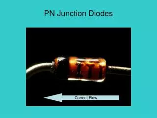
Conclusion • A p–n junction diode allows electric charges to flow in one direction, but not in the opposite direction; negative charges (electrons) can easily flow through the junction from n to p but not from p to n, and the reverse is true for holes.
References • CircuitBread – YouTube Channel • ALL ABOUT ELECTRONICS– YouTube Channel • The science works – YouTube Channel • Electrical4U – YouTube Channel