Digital Logic Circuits (Part 2)
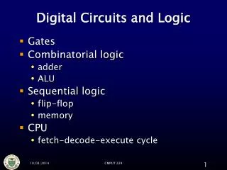
Digital Logic Circuits (Part 2). Computer Architecture. Implementing DeMux in MultiSIM. MultiSIM does not include a classical DeMux It includes a generic decoder ( DCD_2TO4 , DCD_3TO8 , and DCD_4TO16 ) that can be adapted to operate as a DEMUX as shown below:

Digital Logic Circuits (Part 2)
E N D
Presentation Transcript
Digital Logic Circuits(Part 2) Computer Architecture
Implementing DeMux in MultiSIM • MultiSIM does not include a classical DeMux • It includes a generic decoder (DCD_2TO4, DCD_3TO8, and DCD_4TO16) that can be adapted to operate as a DEMUX as shown below: • Basically need to invert the input and the outputs to/from DCD_2TO4
Timing • Gates take time to work • Outputs don’t stabilize for some time • Stabilization time is usually in nanoseconds • Gate delays compound in circuits • Final output is not ready until all gates are stable • Propagation delay • Time taken for changes at the input to propagate to output • Typically, the longest path from input to output • This is often called the “critical path” in a circuit
Example A A•B 2ns A•B•C•D B 2ns C 2ns C•D D Total delay = 4ns
Timing Diagrams • Illustrate change in inputs & outputs in a circuit with respect to time • In the form of a graph • Time on X-axis • Selected inputs / outputs on the Y-axis
Timing Diagram Example A A•B 2ns A•B•C B 2ns C A B C A.B A.B.C 2ns 4ns 6ns 8ns
Mind Bender • What is the output from this circuit when • Input C transitions from 1→0 • Input C transitions from 0→1 C 2ns 1ns • This is an Edge detection logic circuit
Clocks • Delays require careful timing • Otherwise results will be incorrect or garbled • Particularly when multiple inputs are to be processed • I/O is synchronized using a Clock • Clock is a alternating sequence of 1 and 0 • With a given periodicity or frequency • Frequency = 1/Period • Frequency is determined by the gate delays and circuit complexity 1 0
Clock Example • Clocked I/O • Minimum clock period = 4ns • Maximum Frequency = 1/4ns = 250 MHz A 2ns A•B•C Clock 2ns 2ns B 4 ns
Triggering • Clocks transitions are used in different ways • Level triggering • When clock is in a given state • Edge triggering • Raising edge triggered • When the clock is in transition from 0 → 1 • Falling edge triggered • When the clock is in transition from 1 → 0 Rising edge Falling edge Clock
Latches • Latches maintain state • Can be set to a specific value • Output of latches does not change even after Inputs change to 0! • Fundamental units for storage • Building blocks for memory • Latches always store data when the clock is at a fixed level • Hence they are also called as level triggered device
Set-Reset (SR) Latch S R Q 0 0 No change 1 0 1 0 1 0 1 1 Unstable S Q Q R
Clocked S-R Latch • Latch stores (or changes) value only when clock is high • Clock must be at logic level 1 to store data in the latch. • Data can be read at any time S Q Clock / Enable Q R
D-Latch • Advantages over S-R Latch • Single input to store 1 or 0 • Avoid spurious input of S=1 and R=1 D Q Clock / Enable Q
D-Flip Flop • An edge triggered D-Latch is a D-Flip Flop D Q Clock Q • Stores data only on raising edge • Changes at input at other times is ignored • Suitable clock frequency permits data to be stored only after inputs have settled • Data can be read at any time!
Abstract Representations Q Q D D CK CK D-Latch (Positive Level Triggered) D-Flip Flop (Rising Edge Triggered) Q D Q D CK CK D-Flip Flop (Falling Edge Triggered) D-Latch (Negative Level Triggered)
Representations in MultiSIM Positive Edge Triggered D-Latch. Clock must be tied to EN input. Positive Edge Triggered D-Flip Flop. Clock input is labeled CLK.
Asserted: Terminology • Flip Flops use positive or negative logic • Same concept applies to other devices • In order to ease discussion the term “asserted” is used • Positive logic • A “1” triggers the working of the device • Negative logic • A “0” triggers the working of the device
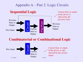
Sequential Logic Circuits • Involve one or more memory elements • Output depends on value in memory element • Typically based on earlier computations or history • Opposite of combinatory logic circuits • Also known as Combinatorial logic circuits • Circuits we have been dealing with so far • Does not include a memory element • Outputs depend purely on primary inputs
Typical Sequential Circuits • Clocks control timings • Ensure values are not stored when they are transient • Have to wait for the signals to stabilize • State elements store values between computations Memory Elements Memory Elements Combinational Logic Combinational Logic
Circuit to read a Bit Q Q Q Q D D D D CK CK CK CK • Given 4 Flip Flops, develop a logic circuit to select and read a given Flip Flop. 4 X 1 Multiplexer Select Lines Output
Circuit to write a Bit Q D CK Q D CK Q D CK Q D CK • Given 4 Flip Flops, develop a logic circuit to select and change data in a given Flip Flop. Input 1X4 De-Mux Clock to trigger one of the D FFs to store the input bit Select Lines
Word • A fixed number of D-Flip Flops • Usually powers of 2 (2, 4, 8, 16, 32, 64) • Operate as a single unit • Store/Read n-bits at a time D0 D1 D2 D3 Q Q Q Q D D D D CK CK CK CK Q0 Q3 Q1 Q2
Reading & Writing Words • A fixed number of D-Flip Flops I2 I1 I3 DeMux DFF DFF DFF DFF DFF DFF S0 Mux #1 Mux #2 Mux #3 O2 O1 O3 CLK RD (1=Read, O=Write)
Random Access Memory (RAM) • RAM is the common form of main memory that is used to store data and programs in modern computers. • It is typically designed as a collection of flip flops as shown in the previous slide • However fabrication technology is different to reduce cost and improve transistor densities • Terminology: • Lines that carry input or output data are referred to as data lines or data bus • The select lines associated with the Mux and DeMux are called the address bus • The selection data is called address • In programming terminology it is called a pointer or a reference.