Download

1 / 16
160 likes | 244 Views
A Fast Evaluation of Power Delivery System Input Impedance of Printed Circuit Boards with Decoupling Capacitors. Jin Zhao (jzhao@sigrity.com) Sigrity Inc. Santa Clara, CA 95051 Om P. Mandhana (Om.Mandhana@freescale.com) Freescale Semiconductor, Austin, TX 78729 October 2004

E N D
A Fast Evaluation of Power Delivery System Input Impedance of Printed Circuit Boards with Decoupling Capacitors Jin Zhao (jzhao@sigrity.com) Sigrity Inc. Santa Clara, CA 95051 Om P. Mandhana (Om.Mandhana@freescale.com) Freescale Semiconductor, Austin, TX 78729 October 2004 EPEP 2004, Portland Oregon
Content • Introduction • Applied Methodology • Application Examples • Conclusion EPEP 2004, Portland Oregon
Introduction • A noise-free, stable power delivery system is required for high speed system • Hundreds of decoupling capacitors are placed on PCB to satisfy the requirement • Efficiently selecting and placing decoupling capacitors on board is a critical task for power integrity analysis and design EPEP 2004, Portland Oregon
On-die Interconnection Package or Substrate Printed Circuit Board VRM on PCB IC CKTs On-board Decaps On-die Decaps On-package Decaps Traditional Approach • Whole system has been represented as multi-stage lumped circuits • As frequency increases, the wave propagation effects within the board structure must be considered in the analysis and design of a PDS EPEP 2004, Portland Oregon
On-die Interconnection Package or Substrate Printed Circuit Board VRM on PCB IC CKTs On-board Decaps On-die Decaps On-package Decaps Applied Methodology Multiple port network Representing Printed Circuit Board Lumped Circuit model Traditional approach New approach EPEP 2004, Portland Oregon
Commercial Field Solver Applied Methodology (cont) Real physical board with pre-selected locations of VRM, decoupling capacitors, and interested IC chip locations Multiple port network Representing Printed Circuit Board Multiple ports corresponding to VRM, decoupling capacitors and interested IC chip locations EPEP 2004, Portland Oregon
Applied Methodology (cont) Multiple port network Representing Printed Circuit Board An impedance matrix can be used to represent the network Multiple ports corresponding to VRM, decoupling capacitors and interested IC chip locations These multiple ports can be divided into two groups: Ports with no termination (open), and Ports terminated with loads EPEP 2004, Portland Oregon
Applied Methodology (cont) Impedance matrix can be expressed as For those ports terminated with a loading, one has The resultant input impedance matrix (at the IC locations) can be calculated as EPEP 2004, Portland Oregon
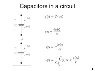
Applied Methodology (cont) Challenges: • Involves large matrix inverse with several large matrix multiplications at every frequency point • Very time consuming as the number of decoupling capacitors placed on board increases • As the impedance of a decoupling capacitor, which depends on the capacitance (C), equivalent series resistance (ESR) and equivalent series inductance (ESL), is included in the matrix operations, ITERATIVELY selecting a decoupling capacitor of appropriate C, ESR and ESL to optimize the power delivery system performance becomes a time consuming process. EPEP 2004, Portland Oregon
Applied Methodology (cont) Admittance Matrix Approach The power ground admittance matrix with some decoupling capacitors mounted on board can be easily calculated by adding the admittance of the decoupling capacitor to the corresponding diagonal entry in the original power ground admittance matrix without any decoupling capacitors mounted on board If no decoupling capacitor mounted at a port, the corresponding entry in the second matrix is 0. EPEP 2004, Portland Oregon
U17 Edge Connector For board power supply Application Example A six layer printed circuit board There are 0.22uF x 8 decoupling capacitors mounted on the upper side There are 0.01uF x 20 and 0.1uF x 8 decaps mounted on the lower side EPEP 2004, Portland Oregon
Application Example (cont) Upper side of the board, U17 is the interested location of power and ground. C21~C28 are eight 0.22 uF decoupling capacitors mounted on board. EPEP 2004, Portland Oregon
Application Example (cont) Lower side of the board, C1~C20 are twenty 0.01 uF decoupling capacitors, C29~C36 are eight 1.0 uF decoupling capacitors mounted on board. EPEP 2004, Portland Oregon
Application Example (cont) Input impedance with and without decoupling capacitors mounted on board EPEP 2004, Portland Oregon
Application Example (cont) Input impedance obtained from commercial software and admittance approach EPEP 2004, Portland Oregon
Conclusion • A fast power ground input impedance evaluation methodology for the printed circuit board with decoupling capacitor placement study is presented. • The admittance approach can accurately estimate the power and ground input impedance up to gigahertz frequency range, which is typically high enough for board level power delivery system analysis and design with targeting of decoupling capacitor placement study. EPEP 2004, Portland Oregon