Download
1 / 48
600 likes | 1.28k Views
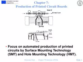
Printed Circuit Boards. Etching and Soldering. Process Outline. General Introduction Creating the PCB Populating the board Soldering Conclusion. General Introduction . We use a heat-transfer resist material Process is best for single-sided boards

E N D
Printed Circuit Boards Etching and Soldering
Process Outline • General Introduction • Creating the PCB • Populating the board • Soldering • Conclusion
General Introduction • We use a heat-transfer resist material • Process is best for single-sided boards • Double-sided boards are possible but difficult • Good results are likely if you follow process and take care to keep materials clean • Trace widths should be ≥ 10 mils
Creating a PC Board • Generate Artwork • Prepare the PCB board material • Transfer resist material to board • Etch the exposed copper • Tin the traces • Drill holes for components
Generate Artwork: Preparation • First print schematics and board layout with components for reference during construction • Your artwork for the PCB image should be in a standard format printable from EE computers, or printed from an EE computer that has the layout software installed • Digital Lab is not a good place to print artwork
Generate Artwork: Printing 1 • Use a printer you can control (so no other lab users will interfere) • Mark the page for re-orientation later
Generate Artwork: Printing 2 • Print on regular paper (Solder layer only!) • Remember the leading edge that came out of the printer first
Generate Artwork: Printing 3 • Cut blue paper slightly larger than PCB image • Do not touch frosty side, keeping it clean and scratch-free increases transfer quality • Place blue paper over the image you just printed, frosty side up • Tape along the full width of the leading edge only • Overlap tape as little as possible
Generate Artwork: Printing 4 • Re-orient paper in printer again • Align mark to original position • Print solder layer again
Generate Artwork: Printing 5 • Artwork is now printed on blue paper • Laser toner will act like glue to bond blue resist material to copper board • Heat will transfer image to PCB
PCB Prep: Cutting & Cleaning 1 • Cut board to size • Boards larger than a standard iron will be tricky • Raw PCB material will be oxidized and dirty
PCB Prep: Cutting & Cleaning 2 • Remove oxidized layer with steel wool • Use enough pressure to remove oxidation, but not so much to gouge the surface • End with light strokes for smooth finish • Shiny surface on finished board
PCB Prep: Cutting & Cleaning 3 • Wash with soap • Dry with paper towel leaving no residue to dry on board • Do not touch copper surface again
Transfer Artwork: Prep • Place PCB over blue paper • Centered & square to image • Tape down on two corners overlapping tape as little as possible (you’ll have to remove it later)
Transfer Artwork: Ironing 1 • Preheat iron • Iron temp is between Polyester & Rayon • Iron surface has holes • Iron must be moved periodically to prevent cool spots under holes
Transfer Artwork: Ironing 2 • Turn board/paper copper side up and iron on blank white side • Cover entire board with iron at all times • Move iron periodically • Slight pressure on iron ensures full surface area contact • Heat for 5 minutes
Transfer Artwork: Cooling • Hold paper tight and rinse under cold water • Do not allow water to deform paper and prematurely separate it from board • Turn over paper and cool back side • Do you take your coffee with ferric chloride?
Transfer Artwork: Separation • Scrape tape off corners of board • Pick up assembly • Hold board in one hand • Slowly, carefully, peel paper away from board
Transfer Artwork: Inspection • Blue material has transferred to board • Look for damaged traces and repair with touch-up marker • Protect blue lines from being scratched off • Blue lines will protect copper from etchant
Etching: Prep • Drill a hole in an unused corner with the 1.15 drill bit (it is better to drill this hole before the art transfer) • Hold material securely so it doesn’t lift and break the bit • Attach a piece of wire through the hole to act as a leash in the chemical bath • Why shouldn’t we strip the wire?
Etching: Bath 1 • Preheat bath with hot plate, etching is faster at higher temp • Fully submerge PCB into etchant solution • Agitate regularly • Ferric chloride will etch away copper not protected by the blue resist material • One of these baths was previously used by design students, can you guess which?
Etching: Bath 2 • Etching will start at edges and move toward center • Remove from bath when all copper is etched away • Excessive bathing will dissolve traces under resist material after adjacent copper is gone
Etching: Cleanup 1 • Wash with soap • Inspect for remaining unwanted copper, re-bathe if necessary • Disconnect leash wire • Remove resist material with steel wool
Etching: Cleanup 2 • Wash again with soap • Unplug hot plate • Replace cover on bath pan after it cools • Your shiny new PCB is ready to tin
Tinning: Flux • Tinning will coat your traces with solder to protect from oxidation and help in the soldering process • Use highly-active liquid flux, one swab-full is plenty • Cover all traces • Use care, this is highly corrosive – after the tinning process it becomes inert but leftovers and spills are hazardous
Tinning: Soldering 1 • Preheat soldering iron to 700° F • Wet sponge with water • Clean tip periodically by dragging and twisting across damp sponge • Handle iron only by handle, do not touch cradle • Wear safety glasses
Tinning: Soldering 2 • Use solid tin/lead solder • We have already provided flux, so do not use rosin-core solder • A small dot of solder on the tip is all you need for several inches of trace coverage
Tinning: Soldering 3 • The key to soldering is heat transfer • Angle tip for maximum surface area contact • Move iron slowly so it transfers heat as you move • Solder will follow tip and wick on to trace as you move
Tinning: Soldering 4 • Smooth motion with constant contact transfers heat effectively • Retrace over pads to remove surplus solder • Do not “paint” with brushstrokes • Each time you lift the iron it stops transferring heat GOOD BAD!
Tinning: Soldering 5 • Surplus solder left on pads will create drilling problem • Use iron to drag solder back along trace
Tinning: Soldering 6 • Incomplete trace coverage caused by not enough heat (iron moving too fast) or not enough solder • Extra solder can be transferred to another trace by dragging with iron
Tinning: Cleanup • Wash off flux • Turn off Iron • Viola!
Drilling: Prep • If some pads still have solder bumps they will be hard to drill through • Use a pin to poke a divot in the center of the mounded pad so drill bit will start easier • Use the 1.15 bit for large, square, or flat leads • Use the thinner #69 bit for standard wire leads
Drilling: Safety & Accuracy • Wear safety glasses, you don’t want a broken drill bit in your eye! • Line up the bit and try to drill exactly in the center of the pad • Adjust your lighting, viewing angle, and technique to ensure accurate hole locations • Be sure you find all the holes you need to drill – it’s very hard to drill holes after you’ve started inserting components
Drilling: Technique • Centered holes make better solder joints • Holes drilled partially off the pad will make poor solder joints • Sequences of un-centered holes make for difficult insertion of SIP & DIP components • Your PCB is now ready to populate
Populating 1 • Have schematic and component diagrams handy for reference • Lay component across its holes to judge bending points • Use needle-nose pliers to bend leads for easy and tidy insertion
Populating 2 • What’s wrong with this picture? • Components lay flat against board. One is bent nicely, one is not • Be sure to get the proper components in the right places
Populating 3 • Bend leads slightly on underside to hold components in place • A tighter fit is accomplished by bending directly underneath board • Use care bending square LED leads, they are brittle and will fatigue easily. • Watch polarity! Square pads denote Negative terminal or Pin 1 for DIPs
Soldering: Prep • Before you start soldering, double-check your schematic and be sure you have the components placed properly • Use rosin core solder for component soldering • Preheat iron to 700° F • Wet tip of iron with a small dab solder to help conduct heat to component lead and trace (this is not the solder that makes the joint)
Soldering: Process • Heat transfer is the key to soldering • A good solder joint requires all parts reach solder melting temperature • Heat pad and lead together with tip of iron • Apply solder to lead and/or pad, NOT to iron • After solder is applied, wait for temp to equalize before pulling out
Soldering: Inspection – Bad Joints Bad joints: • Too much solder (blobs) • Too little solder or not enough heat (gaps/holes) • Too much heat, uneven heat, or too many heat cycles (frosty, pitted, or non-uniform texture, scorched substrate)
Soldering: Inspection – Good Joints Good solder joints: • Smooth volcano shape • Solder wicks along lead and trace • Uniform shiny surface • Retouch joints only if absolutely necessary • Retouching requires reheating the entire joint
Soldering: Trimming • Make a final inspection to be sure you’ve finished all joints • Trim leads when finished soldering • Wear safety glasses • Snipped leads become projectiles, face away from others
Soldering: Finishing Up • Not quite done yet…Turn off your iron!
Finishing Up • Your finished product… or is it? • There, that’s better
Finished Product • Final working product • Adjust frequency by turning potentiometer
Key things to remember: • Safety first • Keep your materials clean for best transfer results • HEAT is the essential ingredient of tinning and soldering • Take the time to be organized, tidy, and thorough • Remember all of this so you don’t have to bug the lab manager when it’s time to make a PCB!
The End • Thank you for listening, have a good day.