Download
1 / 6
160 likes | 644 Views
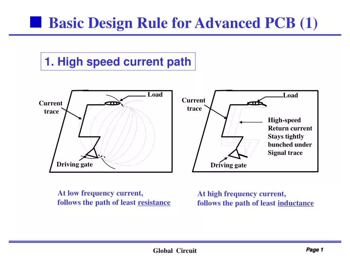
Basic Design Rule for Advanced PCB (1). 1. High speed current path. Load. Load. Current trace. Current trace. High-speed Return current Stays tightly bunched under Signal trace. Driving gate. Driving gate. At low frequency current,

E N D
Basic Design Rule for Advanced PCB (1) 1. High speed current path Load Load Current trace Current trace High-speed Return current Stays tightly bunched under Signal trace Driving gate Driving gate At low frequency current, follows the path of least resistance At high frequency current, follows the path of least inductance Global Circuit
Basic Design Rule for Advanced PCB (2) 2. Induction of slot on Ground plane Return current I.C. I.C. Signal trace Hole clearance on ground plane Equivalent circuit showing inductance in the return path. This inductance is approximately 1nH/cm. Signal trace Return current on ground place Global Circuit
Basic Design Rule for Advanced PCB (3) 3. Trace 3W rule Signal trace w w Via w w w w w w Ground Plane 3W 3W 3W rule is to minimize coupling between trace and signals by providing “clean path” and by aligning the signal flux and the return flux. • Minimize RF fringe between traces • Reduce cross-talk between traces without ground guards Global Circuit
Basic Design Rule for Advanced PCB (4) 4. Inductive & Capacitive Cross-talk Vs Zo Zo Zo source victim Global Circuit
Basic Design Rule for Advanced PCB (5) 5. Concept of transmission line Trace width Micro strip trace Copper thickness h C PCB laminate Dielectric Copper plane Plane Dielectric thickness Micro-strip Plane Plane Dielectric Signal layer Dielectric Signal layer Signal layer Plane Plane Dual Strip-line Strip-line Global Circuit
Basic Design Rule for Advanced PCB (6) 6. Conclusion • High speed PCB design requires consideration of: • Signal Propagation (Ringing & Reflection), • Interaction between signals (Cross-talk, Electro-Magnetic Interference) • High Speed PCB performance needs: • To select suitable material (FR-4, BT, Polyimide, …) • Good process control : • Stack up of layers, especially for multi layers • Uniform and stable impedance (R, L, C) Global Circuit