Download
1 / 9
370 likes | 1.25k Views
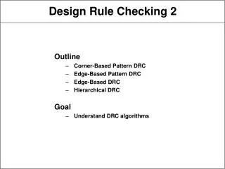
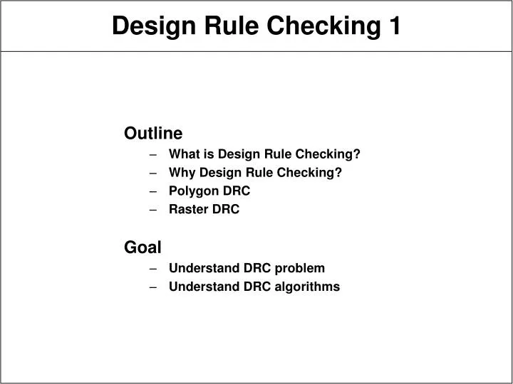
Outline What is Design Rule Checking? Why Design Rule Checking? Polygon DRC Raster DRC Goal Understand DRC problem Understand DRC algorithms. Design Rule Checking 1. Verification that layout geometry is legal obeys set of design rules minimum widths and spacings extensions, overlaps

E N D
Outline What is Design Rule Checking? Why Design Rule Checking? Polygon DRC Raster DRC Goal Understand DRC problem Understand DRC algorithms Design Rule Checking 1
Verification that layout geometry is legal obeys set of design rules minimum widths and spacings extensions, overlaps circuit-dependent rules Goal verify that all rules are met highlight places that rules fail and why use minimum CPU time, memory integrated DRC + layout editor use existing data structures check incrementally What is Design Rule Checking? A Smin = 3 if VAB < 2.5V, Smin = 4 otherwise B
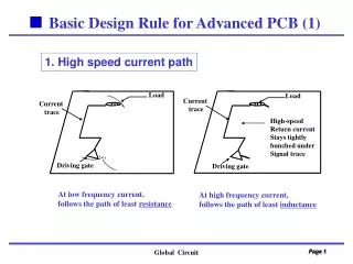
Manufacturing resolution limits can only pattern line widths and spacings above Wmin and Smin limits of photolithography, optics, etc. Manufacturing alignment limits overlay registration varies slightly repeatability of mechanics, sensors Manufacturing disturbances line over/under etching furnace temperature variations particles Layout design rules obey them to get high manufacturing yield a compromise between yield and density rules are local in nature Why Design Rule Checking? vs. vs. vs. vs. vs.
Polygon rectangles as special case most natural representation simple specification of most design rules requires good polygon package Raster at design rule resolution memory hog Tile corner-stitched rectangles, trapezoids good for incremental analysis local connections already stored Edge requires connectivity information minimal memory Geometry Representation 00 10 00 01 11 01 00 10 00
Design rules in terms of boolean operations Met-Met spacing > 3 lambda MetI = inflate(Met, 1.5) Error = MetI MetI Issues inflation of oblique angles robustness of polygon package many tricky cases speed O(nm) operation for n and m-edge polygons memory many auxiliary structures for each edge 2 floats, 5 points in DMW polygon package must merge electrically connected polygons must restrict checks to neighboring polygons avoid O(n2) checks for n polygons Polygon DRC A B A - B A B A B
Find edge intersections O(nm) time for n and m edge polygons use neighborhood check to reduce average to (nlogn) split edges at intersections Walk the edges keeping to edges that are on outside of result polygon use wrap/winding number to compute inside/outside edge crossings of horizontal ray Polygon Operations +1 -1 +1 sum = +1 => inside worst-case
Design rules are local - only check neighborhood objects spread evenly across chip number of neighbors roughly constant Bin sorting divide chip into c x c bins bin points to all objects that intersect it O(1) time to check nearby bins for objects Quad tree search tree - log(n) time to find neighbors Scan line only hold objects within design rule of scan line cutline on n-object chip hits ~sqrt(n) objects n*log(n) time to scan all objects Corner-stitching inherent neighborhood relationships Neighborhood Checking
Scan window over raster d x d for maximum design rule of d units table lookup of d x d window window passes/fails precompute tables one bit per layer layer combinations via bit operations very fast Issues fine grid design rules => large raster I/O time, memory consumption rasterization time use scan line to select polygons to rasterize large d => large tables limited to Manhattan geometry works best on simple MOSIS design rules Raster DRC space 2 ok
Algorithm sort polygons in y and x by upper-left vertex while unrasterized polygons below scanline { move scanline down to next unrasterized polygon or polygon section for each polygon intersecting scanline { rasterize polygon from scanline to scanline + max design rule for each raster pixel in scan line { for each design rule window { check rule report failures } } } Raster DRC