Download
1 / 33
330 likes | 428 Views
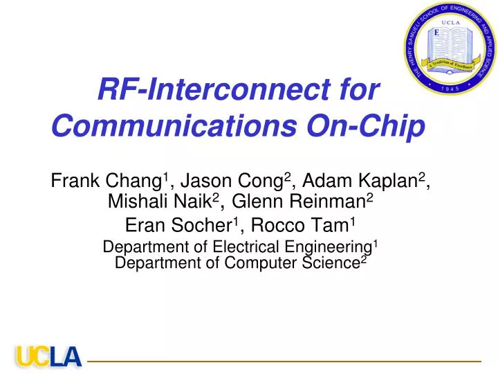
RF-Interconnect for Communications On-Chip. Frank Chang 1 , Jason Cong 2 , Adam Kaplan 2 , Mishali Naik 2 , Glenn Reinman 2 Eran Socher 1 , Rocco Tam 1 Department of Electrical Engineering 1 Department of Computer Science 2. Current Trend in CMP - NoC. 65nm CMOS 80 tile NoC

E N D
RF-Interconnect for Communications On-Chip Frank Chang1, Jason Cong2, Adam Kaplan2, Mishali Naik2, Glenn Reinman2 Eran Socher1, Rocco Tam1 Department of Electrical Engineering1Department of Computer Science2
Current Trend in CMP - NoC 65nm CMOS 80 tile NoC 10X8 2D mesh network-on-chip running @ 4GHz Bisection bandwidth 256GB/s 1 TFLOPS @ 1V about 98W ISSCC 2007: An 80-Tile 1.28TFLOPS Network-on-Chipin 65nm CMOS (Sriram Vangal et al., Intel)
What is The Challenge? Cores would keep shrinking in size but maintain the same operation frequency (2~4GHz) due to thermal constraints More cores would be integrated on the same chip to achieve performance boost through parallelism Performance would be limited by the communicationefficiency between cores and memories on- and off-chip
The Scaling Trend Scaling reduces delay of logic gates but not wires
Traditional Interconnect Units communicate through a parallel bus using voltage signaling (charging and discharging the wire capacitance) Latency is RC limited (~L2) Using CMOS repeaters reduces latency (~L) but does not benefit from scaling Supply no longer scales due to leakage Baseband-only signaling requires extensive equalization Waste of broad bandwidth available from modern CMOS devices (ft>150GHz, fmax>250GHz)
Major Interconnect Issues Latency is large across chip Bandwidth is RC limited (~1Gbps/wire) Communication pattern is fixed Energy consumption is high and not scalable (~10pJ/bit) Future microprocessors may encounter communication congestion and most of the energy will be spent on “talking” instead of computing
How Can RF Help? EM waves travel at the (effective) speed of light (~10ps/mm) Carrier frequencies can be modulated by modern CMOS with high data rates Transmission lines on- or off-chip can guide the waves (RF modulated data) from the transmitter to receiver with recoverable attenuation
RF-Interconnect Concept Data transmit through transmission lines at the speed of light, with less dispersion across the band and less baseband interference data rate is only limited by CMOS mixer modulation speed
RF-I using Multi-band FDMA More bands are used with same modulation speed at each band Higher aggregate data rates can be achieved on the same transmission line
3.6Gbps Multi-drop Multiband Bi-directional RF-I * * World’s 1st Multiband RF-I, Ko & Chang, 2005 ISSCC
Can We Implement RF-I in CMOS? Today’s RF-CMOS circuits are in the wireless communication “sweet spots” of 500MHz-5GHz Insufficient bandwidth for RF-I to be effective! Millimeter-wave CMOS circuits have been developed for 60GHz and recently for 324 GHz bands
CMOS 324GHz Generator • -76dBm before calibration • -46dBm after calibration *Huang, Larocca and Chang, “324GHz CMOS Frequency Generator using Linear Superposition Technique,” pp. 476- 477, 2008 ISSCC
Simultaneous Sub-harmonic Injection Locked mm-Wave Frequency Generation Using sub-harmonic injection-locked VCOs simultaneous lock to one single reference frequency Advantages: Eliminate PLLs Low Power Consumption Small Area Non-linear Harmonic Generator Slave VCOs Master VCO
Sub-harmonic Injection Locked VCO* LC-based VCO core Differential pair for odd harmonic generation Single-ended even harmonic generation Injection locking to high harmonic within locking range of the VCO *Sai-Wang Tam, M.-C. Frank Chang, etc…, "Simultaneous Sub-harmonic Injection-Locked mm-Wave Frequency Generators for Multi-band Communications in CMOS", IEEE RFIC Sym., 2008
RF-I using Amplitude shift-Key (ASK) Modulation • TX: Use transformer couples output of VCO to ASK modulator and use simple modulator to generate RF signal in ASK. • RX: Use self-mixer for envelope detection. Afterwards a simple buffer and Schmitt Trigger recover the signal to rail-to-rail swing.
Differential Transmission Line • Loss of 0.6-1.6 dB/mm Differential TML
RF-I using Amplitude Shift-Key (ASK) Modulation VCO Output: 60GHZ ASK modulated Signal Mixer output 5Gbit/s Data input
Coupling Capacitor 10ps/div Input 500ps/div 50mV/div Output TX in Layer 2 RX in Layer 1 3DIC ASK RF-I Tested at 11Gbps* Output Eye diagram Output versus input Die Photo *Gu and Chang, pp.448-449, 2007 ISSCC (0.33pJ/bit)
Single Channel ASK RF-I Performance Summary • Simple Architecture: One TX VCO, One Mixer, One RX Buffer • No synchronization circuits such as PLL or clock data recovery needed in ASK RF-I • Can expand the same architecture to multi-band RF-I
Interconnect Topology Comparison • Comparison across process technology of… • Traditional RC parallel bus • RF-Interconnect • Optical Interconnect • As process technology scales toward 22nm… • RF-I has lowest latency • RF-I consumes least energy • RF-I has highest data rate density • RF-I is fully compatible with modern CMOS technology 22
Advantages of RF-Interconnects • Latency • Bandwidth • Energy • Reconfigurability
Example: RF-I for CMP NoC Design 10x10 mesh of 5-cycle pipelined routers NoC runs at 2GHz XY/YX routing 64 4GHz 3-wide processor cores containing 8KB L1 Data Cache 8KB L1 Instruction Cache 32 L2 Cache Banks 256KB each Organized as shared NUCA cache 4 Main Memory Interfaces Labeled with + in the figure C C C C C C C C C C C C C C C C C C C C C C C C C C C C C C R R R R R R R R R R R R R R R R R R R R R R R R R R R R R R C C C C C C C C C C C C C C C C C C C C C C C C C C C C C C R R R R R R R R R R R R R R R R R R R R R R R R R R R R R R $ $ $ $ $ $ $ $ $ $ $ $ $ $ $ $ $ $ C C C C C C C C C C C C R R R R R R R R R R R R R R R R R R R R R R R R R R R R R R $ $ $ $ $ $ $ $ $ $ $ $ C C C C C C C C C C C C R R R R R R R R R R R R R R R R R R R R R R R R R R R R R R $ $ $ $ $ $ $ $ $ $ $ $ $ $ $ $ $ $ C C C C C C C C C C C C R R R R R R R R R R R R R R R R R R R R R R R R R R R R R R $ $ $ $ $ $ $ $ $ $ $ $ $ $ $ $ $ $ C C C C C C C C C C C C R R R R R R R R R R R R R R R R R R R R R R R R R R R R R R $ $ $ $ $ $ $ $ $ $ $ $ C C C C C C C C C C C C R R R R R R R R R R R R R R R R R R R R R R R R R R R R R R $ $ $ $ $ $ $ $ $ $ $ $ $ $ $ $ $ $ C C C C C C C C C C C C R R R R R R R R R R R R R R R R R R R R R R R R R R R R R R C C C C C C C C C C C C C C C C C C C C C C C C C C C C C C R R R R R R R R R R R R R R R R R R R R R R R R R R R R R R C C C C C C C C C C C C C C C C C C C C C C C C C C C C C C R R R R R R R R R R R R R R R R R R R R R R R R R R R R R R R (square) = router C (circle) = processor core $ (diamond) = L2 cache bank + (plus) = main memory interface
MORFIC: Mesh Overlaid with RF-InterConnect Shared Z-shaped RF waveguide Organized as 8 bidirectional shortcut links Each direction of each shortcut can transmit simultaneously over shared medium Router A can send a flit to other router A, B to B, … H to H in a single cycle Router labeled X cannot directly send to any router not labeled X E.g. Router B in upper left cannot send to router E in upper right directly However, B in upper left can send to B in upper right, and then north to E using normal mesh link C C E A A D D E B B B B G G H H E A E A F F F F H H C C D D G G LOGICAL ORGANIZATION PHYSICAL ORGANIZATION
MORFIC Results For 256B Total RF-I [HPCA’2008] • 256B RF-I consumes 0.18% silicon overhead on 400mm2 die • RF-I components: 0.13%, Router overhead: 0.05% • Normalized Splash-2 Execution Time and Average Packet Latency Results • Normalized to baseline mesh run-cycles/latency at 1 • Average 13% (max 18%) performance improvement • Average 22% (max 24%) packet latency improvement
The Bad News …Most Interconnect Optimization Techniques May Not be Relevant … • Performance-driven interconnect design based on distributed RC delay model -all 10 versions »Jason Cong, Kwok-Shing Leung, and Dian Zhou, Design Automation Conference 1993, Cited by 141 - Related Articles - Web Search - Library Search • Interconnect design for deep submicron ICs - all 25 versions »J Cong, L He, KY Khoo, CK Koh, Z Pan - Proc. Int. Conf. on Computer Aided Design, 1997 - doi.ieeecomputersociety.orgCited by 139 - Related Articles - Web Search • Efficient algorithms for the minimum shortest path Steiner arborescence problem with applications to … - all 11 versions »Jason Cong, Andrew B. Kahng, and Kwok-Shing Leung, IEEE TRANSACTIONS ON COMPUTER-AIDED DESIGN OF INTEGRATED CIRCUITS AND SYSTEMS, VOL. 17, NO. 1, JANUARY 1998 Cited by 127 - Related Articles - Web Search • Buffer block planning for interconnect-driven floorplanning - all 21 versions »J Cong, T Kong, DZ Pan - Proc. Int. Conf. Computer-Aided Design, 1999 - doi.ieeecomputersociety.orgCited by 130 - Related Articles - Web Search … (from Google Scholar)
Good News -- Plenty of New Problems for Future PhD Students • How many/which routers should be RF-enabled? • How many RF-I ports should each router have? • Dedicated or multiplexed with other ports? • How much RF-I bandwidth to allocate? • Total? Per communicating pair? • Impacts active layer area consumed by RF-I components • Which routing strategy to employ in presence of RF-I express channels? • Dynamic or static allocation of frequency bands to sources/destinations • Dynamic: requires arbitration overhead for channel assignment • Static: may miss opportunity to match changing communication demand • Support of multi-cast
Example: Deadlock: To Avoid or Confront? • South-Last Strategy [Ogras and Marculescu, 2006] • Routes which can lead to circular buffer dependence are forbidden avoids deadlock • Deadlock Detection & Recovery (DDR) • Based on Duato and Pinkston’s theory[Duato and Pinkston 2001] • If deadlock occurs, route all packets in the network on a spare virtual channel • Use deadlock-free XY-routing • Packets entering network after this point may be routed normally
Deadlock Results • South-Last strategy too restrictive • Halves the average realizable performance • Deadlock is best detected and recovered from when it occurs • Detection happens reasonably quickly • Performance during recovery no worse than baseline
Example: RF-I Topology and Bandwidth Optimization • For each channel • Source and destination may be reconfigured via frequency-band reassignment • Can assign variable # of channels to each source, destination pair (s,d) • critical channels given more bandwidth • A flexible means to reconfigure topology PHYSICAL LOGICAL B LOGICAL A
Conclusions • RF-I on CMOS is real • RF-I is a very promising solution to global interconnect bottleneck • Latency • Bandwidth • Energy • Reconfigurability • RF-I introduces many interesting physical and architecture design problems in NoC designs