Download
1 / 68
680 likes | 683 Views
This paper examines the data transmission protocols and challenges faced by particle physics experiments in terms of radiation hardness and device longevity. It discusses the use of optical links in collider experiments and presents predictions and tests for optical link radiation hardness. The paper also explores the radiation hardness of commercial devices and the materials used in light-coupling.

E N D
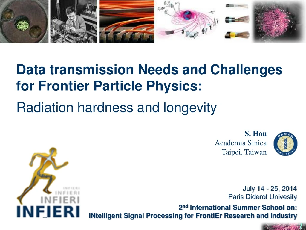
Data transmission Needs and Challenges for Frontier Particle Physics: Radiation hardness and longevity S. Hou Academia Sinica Taipei, Taiwan July 14 - 25, 2014 Paris Diderot Univesity 2nd International Summer School on: INtelligent Signal Processing for FrontIEr Research and Industry
Outline • Introductiondata transfer protocols, low loss fiber innovation • opto-electronics, industrial development • Optical links in collider experiments LHC devices CDF tracker optical link, longevity • Radiation hardness of optical links predictions tests to CDF transmitter tests to VCSELs, PINs • Radiation hardness of commercial devices Light-coupling material VCSEL, Control IC, BER
Introduction:data transfer protocolslow loss fiber innovationopto-electronicsindustrial development
Introduction: data transfer protocols • Internet TCP (Transmission Control Protocol) : • Duplex data transfer, demanding reliability • TCP forwards “packets” of Internet Protocol over networks between hosts • Encapsulated, Telnet, FTP, SMTP, HTTP, … for applications • Computer peripherals, e.g. USB (Universal Serial Bus): • Standardize connection of computer peripherals: keyboards, hard drives .. • Host centric bus with layers of protocols • Detector data acquisition: • Detector measurements are analog signals, • Front-end ADC, multiplexing … real-time data output, no handshape • May require inputs for slow control for clock, setup,
Internet TCP • TCP (Transmission Control Protocol) • Internet communication with three way handshakes • Reliable with data packets ACKnoleged in SEQuence • Acknowledgements indicate delivery of data • Checksums are used to detect corrupted data. • Sequence numbers detect missing, or mis-sequenced data. • Corrupted data is retransmitted after a timeout. • SYN (synchronize sequence numbers) • ISN (initial sequence number)
Computer network with USB • USB (Universal Serial Bus ) “Single Master + Multiple Slaves” • One interface for many devices • Hot pluggable, automatic configuration • Hi-Speed – 4.8 Gbps (USB3) • USB transaction , • strictly defined frame, error checking and handshaking • - Token Packet, header defining what to follow • - Optional Data Packet • - Status Packet, to acknowledge transactions
Fiber optics 1963: Semiconductor laser high threshold (~Amps) Low temp (77K) 1989 Payne et al (U. Southampton) Er-doped fiberamplifier (EDFA) 1969 Alferov (USSR) and Pannish & Hayashi (Bell Labs) Rm Temp, CW, semiconductor lasers Active Devices 1969 Uchida (Nippon Sheet Glass, Japan) Multi-component Selfoc fiber (~100dB/km) 1970 Kapron, Keck, & Maurer (Corning) Low loss Silica fiber (20dB/km) 1974 MacChesney (AT&T) 1dB/km 1966: C. Kao predicted Fiber attenuation low limit 20 dB/km (in 1966, ~1000dB/km), Nobel Prize ‘09 Optical Fibers
Fiber capacity Speeds and capacities of optical core, access networks are being boosted NTT Technical Review
Fiber optical loss • Silica glass fiber: • Low-mass, high bandwidth, little loss over long distance • Absorption Scattering losses (Rayleigh, Raman…) • Bending losses (micro bending) 1st generation, ~1975, 0.8 μm fiber-MM, Laser GaAs 2nd generation, ~1980, 1.3 μm, fiber MM SM, InGaAsP FP-laser 3rd generation, ~1985, 1.55 μm, fiber SM InGaAsP DFB-laser 4th generation, 1996, 1.55μm WDM s
Opto-electronics • Transceivers: • Laser diodes as light source • PIN diodes as photo detector • Driver chip convert electrical signals to optical, and vice versa • Control IC for the application protocols 850-nm VCSELs - for short-distance over multimode fiber 1300-nm VCSELs - for longer-distance communication over single-mode fiber 1550-nm VCSELs - tunable sources for DWDM multiple transmissions over one fiber
Light sources Spontaneous light emission Laser Diodes (LD), Light Emitting Diodes (LED) LED LD has an optical cavity for stimulated emission. Light Amplification by Stimulated Emission of Radiation (LASER)
Photo-detectors • Photo-detector (PD) • converts incident light pulse into electrical signal • - PIN Photo-detector(most common PD in use) • - Avalanche Photo-diode (APD) • PIN diode is operated in the reverse-bias mode • -wide depletion region to create electron-hole pairs • - low junction capacitance allows for very fast switching
Building an eye pattern Eye Diagram on oscilloscope triggered by data clock. • Deterministic jitter: • caused by dispersion in fiber, and • inadequate bandwidth of transceiver components • Random jitter: • caused by thermal noise, shot noise in components Non-Return to Zero (NRZ)
Commercial optical transceivers • telecommunication and computing • 10 Gb/s SFP+ transceivers • 4.8 Gb/s USB3 Active Optical Cable 5 Gbps USB3 10 GB/s SFP+
Chip-on-Board, QSFP of TrueLight • Assembly service to customer • VCSEL, PIN arrays of TrueLight • Lens, driver, circuit provided by customer, • MT ferrule, 4-in 4-out, 40 Gb QSFP optical engine • TX 10 Gb tests • RX 10 Gb tests
Light Peak Technology • Light Peak, Intel technologydelivers high bandwidth starting at 10 Gb/sto mainstream computing and consumer electronics • Lens/Prism :precision PEI molding .. Full acceptance angle 25.4 degree Spherical-aberration free Plano-Convex Hyperbolic Lens Divergence angle 26 – 32 degree VCSELsaperture from t Ø 5 to 20 µm (FOCI prism)
FOCI optical engine functional diagram • VCSEL/PIN: • 850 nm bare die, • 4.8 Gb/s or 10 Gb/s • >0 dBm (1mW) • Optical IC: • VIA Labs V0510, • TSMC 90nm technology • USB-3 protocol, ~60 mW, • 4.8 Gb/s TX/RX driver • + regulator/controller
Optical links in collider experimentsLHC devices CDF tracker optical link, longevity
ATLAS SCT transceiver • Detector data acquisition: • Analog signals digitization (front-end IC, ADC) • data transfer • Front-end INPUT clock, IC configuration • Front-end OUTPUT continuous data transfer 1 RX PIN + DORIC for clock+command 2 TX VCSEL + VDC for data 45o fibre end, mirror to VCSEL, PIN face Opto-flex: Holds VDCs, DORICs, PINs, VCSELs VDC: VCSEL Driver Circuit DORIC: Digital Optical Receiver Integrated Circuit
ATLAS LAr MTX • Similar to CERN VL product, • TOSA + MM fiber, 850nm • Use LOCld, driver of SOS process • Speed 8 Gb/s • Different geo/connector configuration • constrain by LAr geometry TWEPP2012, Liu, SMU
High throughput array OSU prototype, ATLAS Pixel VCSEL array, driver of 130 nm CMOS. 8 channel + 4 spare channels TWEPP2012, Gan, OSU
CDF optical link The 1st optical link in Collider experiment inner tracker • Dense Optical Interface Module • Byte-wide parallel link • 8-bits + clock • 53 Mbyte/sec, BER10-12 • Transmitter on portcard: • Laser-diode array • ASIC driver chip • Receiver on FIB crate : • PIN-diode array • ASIC receiver chip • Multi-mode fiber ribbon
CDF tracker Port Card • Total 128 portcards 5 optical TX each portcard total 570 TX • Transceiver : convert low-voltage differential signals from DAQ to Silicon detector • Digital Data Receiver : Decode 5-bit commands into 10 SVX3D control and calibration • Analog DDR: regulates AVDD for clean frontend operation • Optical transmitter : • 8 data bit + 1 data valid signal to Laser Diode Array to 9-bit parallel optical link
CDF optical link, transmitter assembly • Die-bond / Wire bond • laser-diode array on BeOsubmount • driver chip on substrate • fibers on V-groove • Alignment • fibers to laser emitting facets
CDF optical link, transmitter electronics • InGaAs/InPEdge-emitting laser diode array • 1550 nm wavelength • 12-ch diode array, 250 m pitch • Bare die power, 1 mW/ch @20mA • Insertion to fiber: 200 ~ 800 W/ch • Custom made by Chunghwa Telecom • biCMOSASIC driver • bipolar transistors, AMS 0.8 m process • 9-channels • Inputs: Diff. ECL or LVDS • differential 100 mV • Enable by TTL low • Output light: adjustable by • ~2mA/0.1V • At Vcc-VLD=3V, 20mA/ch
CDF optical link, receiver module • InGaAs/InPPIN diode • 12-ch array, 1550 nm • by TL, Chunghwa Telecom. • Operation condition : • light on: 50 ~ 800 W • light off: 10 W • 1.1 W/module • Outputs: • 9 independent diff. ECL • Die-bond / Wire bond • PIN-diode array on Al2O3submount • driver chip on substrate • fibers on V-groove to PIN diodes
CDF optical transmitter test • Inputs: • ECL or LVDS signal • TTL-enable Light by O/E probe Input ECL TTL enable
CDF edge-emitting laser, characteristics • Laser light at I,V and Temperature • I-V approximately linear • Duty cycle • stable output to input 50% • Linear to temperature Temp (oC)
CDF optical transmitter production uniformity • Quality analysis • light measured from pigtails at 30oC • wide deviation channel-by-channel • mainly due to insertion efficiency • Span within ~400 W • ~72 W to the mean/module
CDF optical receiver responses • Rere • Receiver connected to a Transmitter • Light power chosen for • wide distribution • Light pulse width are consistent • Receiver ECL outputs • by a Tektronix diff. probe • Consistent duty cycles in favored operation range (2.8~3.2V) • Saturates for high light level
CDF optical link, Bit-Error-Rate test • BERT by Fermilab • PC ISAbus interface • Tbert, Rbert- test boards • At 63 MHz, • minimum BER 10 –12 • Burn-in • 3-days on ASICs, diodes • 1-day BERT • reject devices infant mortality • bad components fail quickly
Optical transmitter, accelerated ageing • Transmitters biased at 60oC for 330 days • Accelerating factor , Arrhenius eq. • Ea= 0.4 eV for GaAs • F=15 to T1= +6oC • Wear-out degradation • ~10% at 60oC, no failure • corresponding to • CDF operation at +6oC • for 15 years
CDF optical link longevity • Commissioning was problematic: • ~ a dozen bit-error channels • temperature from Room to 6oC • increased light power • wider width NRZ bit locku • loosened connectors • permanent loss • Optical link bit-error • after commissioning ~ 2% • 10 years operation • ageing, radiation damage • outer tracker (ISL) • stay at ~2% • inner most (SVX-II) • increase to a total ~ 4% Fraction of silicon ladders
Radiation hardnessof optical links PredictionsTests to CDF transmitterTests to VCSELs, PINs
Radiation damage • Interaction of radiation with material • Gamma Total Ionizing Dose (TID), SEU • Charge hadron, neutron NIEL, degradation, SEU • Ionization: • charge trapped in oxide or at interface • Displacement:(NIEL, non-ionizing energy loss ) • atoms can be removed from their initial crystal lattice positions • defect in components • degradation, annealing • Single event effect (SEE) • transient, corrupted bits, • IC functional interrupt
NEIL in Si damage function • Hypothesis: Damage parameters scale with the NIEL • 1 MeV neutron equivalent damage RD50
NIEL of Proton in GaAs • Proton damage to GaAs LED, Solar Cell • does not agree with beam tests J.H. Warner et al., IEEE TNS 51, 2887 (2004) C. Poivey, EPFL Space Center 9th , Jun 2009
Radiation Field in ATLAS • Exposure to radiation from pp collisions • mainly pions • neutrons (hadrons interact with material) • 10 years operation • TID > 100 kGy • NIEL φeq > 1015 1 MeV n/cm-2
Radiation fields @LHC, SLHC • Fluence expressed for 1 MeV neutron equivalent of the NIEL (Non-Ionizing Energy Loss) calculations NIEL factors for Neutrons [MeV] 1 20 GaAs [keV cm2/g] 0.55 2.3 Si [keV cm2/g] 1.8 NIEL factors for Protons [MeV] 30 70 200 GaAs [keV cm2/g] 4.03 3.64 3.93 Si [keV cm2/g] 4.78 3.16 1.94 • [Summers, IEEE NS. 40 1372 (1993)] • Radiation level @LHC/SLHC
CDF Radiation Measurement Radiation from pˉp Collisions TLD measurements + model r = radius to the beam α ~1.5 in barrel region Locations of TLDs (Thermal Luminescent Dosimeters) R.J Tesarek IEEE NSS 2003
CDF Radiation estimation • By MC for distributions of particles in • pˉp Collisions • Dose to fluence conversion: • 1 Gy = 100 Rad = 3.8x10⁹ MIPs/cm2 • (Silicon tracker is specified for 2 MRad) • Radiation tolerance: • Optical Transmitter required for • 200 kRad 7.6x12 MIPs/cm2 • Dose rate at the optical Transmitter • r=15 cm, dose rate = 17 Rad/pb-1 • 200 kRad 11.8 fb-1in the beam • Team tests with fixed energy hadrons • dose scaled by dE/dx • 1 Gy = 2.1x10⁹ p(200MeV)/cm2 • = 5.4x10⁸ p( 30MeV)/cm2
Radiation tolerance of laser diodes • Displacement, NEIL • Light degradation, partial recovery by annealing • Increasing threshold current • Edge-emitting Fabry-Peror laser • Active optical cavity, typically • ~500x50x10 μm3 • VCSEL • very small active volume • ~∅20x10 μm3 • very high Rad-hardness
Radiation damage to PIN photo-detectors • Displacement, NEIL • Increase in leakage Ileak • decrease in responsivityIphoto • Damage pattern varies • Si Epitaxial PIN • GaAs PIN • Faster PIN • smaller device, • Higher rad-hardness
Proton beam tests on CDF transmitter • Cyclotron 30 MeV protons at INER • Measuring L, temperature at DC mode • fiber connection out of beam area
Proton irradiation to CDF transmitter CDF edge-emitting type laser • Flux rate dependence not obvious • IUCF 200 MeV protons at 3 flux rate • Pulsed by 50% duty cycle signals • flux- = 3.4 E9, 11.5 E9, 29.2 E9/cm2sec • fluence= 4.3 E12, 12.8 E12, 30.0 E12/cm2 • Slow annealing after • IUCF 200 MeV protons • Transmitter at DC mode • Total fluence 1.2E13 /cm2 • 8 hours annealing 8hrs annealing