Download
1 / 61
630 likes | 801 Views
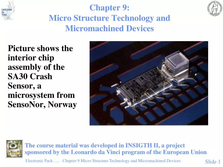
Chapter 9: Micro Structure Technology and Micromachined Devices. Picture shows the interior chip assembly of the S A30 Crash Sensor, a microsystem from SensoNor, Norway.

E N D
Chapter 9:Micro Structure Technology andMicromachined Devices Picture shows the interior chip assembly of the SA30 Crash Sensor, a microsystem from SensoNor, Norway The course material was developed in INSIGTH II, a project sponsored by the Leonardo da Vinci program of the European Union Electronic Pack….. Chapter 9 Micro Structure Technology and Micromachined Devices
Definitions • MICRO STRUCTURE TECHNOLOGY can be defined as a group of three-dimensional micromachining techniques enabling feature dimensions with accuracy in the micrometer range. • MICROMACHINED DEVICES can be defined as devices made by Micro Structure Technology. • These micromachining techniques are mainly based upon batch organised microelectronic process technology, either directly adapted techniques like photolithographics, or modified techniques such as anisotropic etching techniques. • Some micromachining techniques are specially developed for this field, e.g., anodic bonding of micromachined devices. Electronic Pack….. Chapter 9 Micro Structure Technology and Micromachined Devices
Example: SP80 Pressure Sensor • Developed at SINTEF (earlier Center for Industrial Research), Norway and manufactured by Capto as (earlier SensoNor AS, earlier ame), Borre, Norway. • This sensor visualises the main features and limitations of micromechanical sensors, and points out pressure sensing as a main application for these kinds of sensors. Electronic Pack….. Chapter 9 Micro Structure Technology and Micromachined Devices
SP80 Principal Design • A piezoresistive integrated pressure sensor with the pressure-sensitive diaphragm micromachined in a silicon chip by anisotropic etching. • Ion implanted piezoresistors in a full Wheatstone bridge configuration as the electronic sensing element. • Temperature measuring resistor and a heating resistor are implanted on the same chip, to compensate or thermostat the chip to minimise thermal drifts. • By varying the area and the thickness of the diaphragm, pressure ranges from 0.5 Bar full scale pressure up to 60 Bar full scale pressure can be achieved • Packaged in a transistor header • Main application areas are within general instrumentation, metrology and aerospace application. Electronic Pack….. Chapter 9 Micro Structure Technology and Micromachined Devices
The SP80 Silicon Chip Set - Drawing • Consists of diaphragm chip sealed to a support chip which is mounted on top of a glass tubing acting as a mounting stand as well as a pressure port. Electronic Pack….. Chapter 9 Micro Structure Technology and Micromachined Devices
The SP80 Silicon Chip Set - Picture • Consists of diaphragm chip sealed to a support chip which is mounted on top of a glass tubing acting as a mounting stand as well as a pressure port. Electronic Pack….. Chapter 9 Micro Structure Technology and Micromachined Devices
The size is 4*4 mm, thickness approximately 0.3 mm, the diaphragm area is typical 2*2 mm and the diaphragm thickness is typical 30 micrometers. The diaphragm is manufactured by stripping off the surface oxide of the silicon wafer by means photolithographic technique in the areas we want the diaphragm cavity. Then the wafer is etched in an anisotropic etching solution with the remaining oxide as masking film. This etching solution attacks the single crystal silicon with different speed in the different crystal directions. The etch is extremely slow in the <1-1-1> direction: The etch is therefore stopped towards the (1-1-1) planes. The chip material is (1-0-0) silicon Therefore, the etch cavity is surrounded by four (1-1-1) planes which have an angle of inclination of 54.7 degrees relative to the (1-0-0) surface plane, rendering a cavity with four sloped walls. Dimensions and Processing Electronic Pack….. Chapter 9 Micro Structure Technology and Micromachined Devices
Cross-sectioned view of the SP80 Pressure Sensor packaged in a transistor header. SP80 Package Electronic Pack….. Chapter 9 Micro Structure Technology and Micromachined Devices
Cross-sectioned view of the SP80 Pressure Sensor packaged in a transistor header with a top chip containing a vacuum reference chamber. SP80 Package, continued Electronic Pack….. Chapter 9 Micro Structure Technology and Micromachined Devices
The SP80 schematic consists of 4 ion implanted piezoresistors in a full Wheatstone bridge configuration as the electronic sensing element. In addition, a temperature measuring resistor and a heating resistor are implanted on the same chip, to compensate or thermostat the chip to minimise thermal drifts. SP80 Schematic Electronic Pack….. Chapter 9 Micro Structure Technology and Micromachined Devices
Comment: The Norwegian coin is approximately the size of Ø10 mm Picture of SP80 in Transistor Package Electronic Pack….. Chapter 9 Micro Structure Technology and Micromachined Devices
Main Features of SP80 • Low non-linearity ( < +- 0.1% ) • Negligible hysteresis ( < +- 0.005% of full scale output ) • Low long term drift ( typical less than 0.1% per year ) • Active thermal compensation by utilising the on-the-chip heating resistor. • Small size. Electronic Pack….. Chapter 9 Micro Structure Technology and Micromachined Devices
Drawbacks of SP80 • Reference pressure medium must be non-conducting and non-corrosive to be compatible with the on-chip sensing elements and electronics. • Safe overload is limited to 3 times rated pressure as no mechanical overload stop is implemented. • The devices have no normalised output signal. Each device has to be individually calibrated when system installed. • Temperature range is limited (-55 - +125 °C) and uncompensated thermal sensitivity drift is relative high ( = -0.2%/°C). Electronic Pack….. Chapter 9 Micro Structure Technology and Micromachined Devices
Applications for Micromachined Sensors and Microsystems: • The biomedical market • Blood pressure sensors • The space, defence and avionics markets • Accelerometers for rocket navigation • Micro gravity sensor • Gyroscopes for navigation • The agriculture electronics market • Automotive sensors used in tractors, harvesters etc. • The off-shore oil exploitation market • High pressure measurement in oil wells • Sea wave sensor • The automotive market • Acceleration microsystems for air bag systems • Tire pressure microsystems • The data and peripheral market • Disk drive write and read heads • The consumer market • Photo diodes in cameras • Level measurement in white goods appliances. Electronic Pack….. Chapter 9 Micro Structure Technology and Micromachined Devices
Top10 Success Factors • 1. Batch organised processing technology • 2. Microelectronics manufacturing infrastructure • 3. Research results from solid state technology and other related fields of microelectronics • 4. Micromachining • 5. Wafer and chip bonding • 6. Mechanical material characteristics • 7. Sensor effects • 8. Actuator functions • 9. Integrated electronics • 10. Combination of features Electronic Pack….. Chapter 9 Micro Structure Technology and Micromachined Devices
Bottom10 Limiting Factors 1. Slow market acceptance 2. Low production volumes 3. Immature industrial infrastructure 4. Poor reliability 5. Complex designs and processes 6. Immature processing technology 7. Immature packaging and interconnection technologies 8. Limited research resources 9. Limited human resources 10. High costs Electronic Pack….. Chapter 9 Micro Structure Technology and Micromachined Devices
Milestones in the Planar Silicon Processing Technology (and some other related breakthroughs): • 1890: Punched cards invented • 1939: Vacuum tubes and mechanical computing • 1948: The invention of the transistor • 1959: The invention of the planar silicon processing • 1959: The invention of the integrated circuit • 1964: Mainframe computing • 1971: The invention of the microprocessor • 1981: introduction of personal computers • 1985: 1 Megabit random-access-memory chips available • 1991: 64 Megabit random-access-memory chips available • 1994: Internet in widespread use • 1994: 256 Megabit random-access-memory chips available • 1995: Microprocessors with more than 3 million transistors available • 2000: Microprocessors with more than 100 million transistors available • 2005: 1 Gigabit random-access-memory chips available • 2006: Digital consumerisation (Video on mobile phones etc) • 2007: The Intel Itanium microprocessor with 1.2 billions transistors. • 2008: 4 Gigabit random-access-memory chips available Electronic Pack….. Chapter 9 Micro Structure Technology and Micromachined Devices
Manufacturers of Micromechanical Devices • The industry structure is highly diversified both in size, technological basis and organisation type. • Traditional sensor manufacturers have seen micromechanical sensors as a natural expansion of their technological basis, and have taken up research and production of these sensors as a part of their activity. • Semiconductor companies have entered this market as an expansion of their integrated circuit activity, since they already have most of the needed equipment and the appropriate marketing channels. • System companies or original equipment manufacturers which see micromechanical devices as a way to boost their systems. • "Start ups", companies having micromechanical devices as their main business idea. • There are of course companies that does not fit into any of these types and some are someplace in between these types. Electronic Pack….. Chapter 9 Micro Structure Technology and Micromachined Devices
Manufacturers • USA: • Honeywell, Microswitch, SenSym, IC Sensors, Motorola, Delco, Foxboro/ICT, Endevco, Kulite, Lucas/NovaSensor, Michigan Microsensors • Japan: • Hitachi, Toshiba, NEC, Yokagawa Hokushin, Toyota Motor Company • Europe: • Germany: Infineon, Bosch, • The Netherlands: Philips, Microtel, Xensor Integration • UK: Druck • Switzerland: Keller, Kistler • Finland: Vaisala • Sweden: Radi Medical Systems • Norway: SensoNor Electronic Pack….. Chapter 9 Micro Structure Technology and Micromachined Devices
Research Centers • USA • Stanford University, Case Western Reserve University, University of Michigan, University of California at Berkeley, University of Wisconsin, MIT • Japan: • Tohoku University, Kyoto University, Fudan University, • Europe: • The Netherlands: Delft University, Twente University • Belgium: IMEC, Catholic Un of Leuven • Switzerland: University of Neuchâtel, CSEM • Germany: Fraunhofer Institute, IFT Munich, Fraunhofer Institute, IMT Itzehoe, Techn. Un of Berlin • Denmark: Techn. Un of Denmark • Finland: VTT • Sweden: Uppsala University, KTH/Acreo • Norway: SINTEF Electronic Pack….. Chapter 9 Micro Structure Technology and Micromachined Devices
Batch Processes Adapted from Microelectronics/IC Technology with no or Minor Modifications • Photolithography • Spin coating • Etching techniques • Diffusion of dopants • Implantation • Epitaxy • Chemical vapour deposition (CVD) • Thin film technology • Thick film technology Electronic Pack….. Chapter 9 Micro Structure Technology and Micromachined Devices
Batch Processes Modifiedfrom Microelectronics/IC Technology Processes • Double-sided photolithography • Wafer fusion bonding • LIGA and LIGA-like techniques • Laser micromachining Electronic Pack….. Chapter 9 Micro Structure Technology and Micromachined Devices
Batch Processes Adapted or Modified from Other Technologies than Microelectronics/IC Technology • Micro stereo lithography • Micro electro discharge machining Electronic Pack….. Chapter 9 Micro Structure Technology and Micromachined Devices
Batch Processes Mainly Developed for Micromachined Devices • Bulk micromachining • Surface micromachining • Anodic wafer bonding • Fusion bonding (Direct bonding)These technologies will be commented on the following slides Electronic Pack….. Chapter 9 Micro Structure Technology and Micromachined Devices
Bulk Micromachining in Silicon • Bulk Micromachining in Silicon is here defined as three-dimensional micromachining in single crystal silicon by means of photolithographic etching techniques. • It is also called Bulk Micromechanics in Silicon or Silicon Micromachining • To understand this technology, some basic insight in single crystal silicon is needed Electronic Pack….. Chapter 9 Micro Structure Technology and Micromachined Devices
Crystal Structure of Single Crystal Silicon • It is a face-centered cubic structure (diamond structure) with two atoms associated with each lattice point of the unit cube. One atom is located in position with xyz coordinates (0, 0, 0), the other in position (a/4, a/4, a/4), a being the basic unit cell length. Electronic Pack….. Chapter 9 Micro Structure Technology and Micromachined Devices
Miller Indices for a Plane in a Crystal The orientation of of different crystal planes in the basic unit cell can be described by the Miller indices (hkl) between parentheses with each plane defined by a vector description (hx + ky + lz) of the direction perpendicular to that plane. This is related to a coordinate system oriented in parallel with the side edges of the basic cell, with the Miller indices reduced to the smallest possible integers with the same ratio. Electronic Pack….. Chapter 9 Micro Structure Technology and Micromachined Devices
Important Crystal Planes in the Silicon Crystal • (100), (110) and (111) are the three most important crystal planes of the silicon crystal structure. Electronic Pack….. Chapter 9 Micro Structure Technology and Micromachined Devices
Silicon as a Mechanical Material Electronic Pack….. Chapter 9 Micro Structure Technology and Micromachined Devices
Silicon as an Electronic Material Electronic Pack….. Chapter 9 Micro Structure Technology and Micromachined Devices
Principles of Micromachining in Silicon • Micromechanics in silicon is here defined as three-dimensional micromachining in single crystal silicon by means of photolithographic etching techniques. • This definition covers most techniques used to make micromechanical sensors, although in some cases additive structures such as polysilicon and silicon dioxide also have been micromachined by selective etching techniques, and in some cases mechanical drilling or other machining methods are used. Electronic Pack….. Chapter 9 Micro Structure Technology and Micromachined Devices
Wet Chemical Etching of Silicon using Alkaline Etchants • The fundamental reactions are electrochemical in nature. • Holes are injected from the etching solution into the silicon and Si-atoms are ionized to Si+. • Hydroxyl (OH-) from the etching solution reacts with Si+ to hydrated silicon. • Hydrated silicon reacts with a complexing agent in the etching solution to form a soluble reaction product. • The soluble reaction product is dissolved into the etching solution and carried away from the etching site on the silicon surface into the solution. • All in all, silicon is etched and the reactant products are diluted into the etching solution. Electronic Pack….. Chapter 9 Micro Structure Technology and Micromachined Devices
Isotropic Etching of Silicon • Typical wet isotropic silicon etches are either organic or inorganic acids such as acetic acid (CH3COOH) or hydrogenfluorid (HF) or mixtures together with water. Often a complexing agent is needed transforming the oxidized product into soluble species. • By using selective etching techniques in combination with etching time some sort of dimensional control of the etched structure can be obtained. By using spray etching, agitation or light enhanced etching preferred etching directions can be obtained. • Generally, dimensional accuracy below approximately 30 µmeters are very hard to achieve, making wet isotropic etching a less favourable and less used method for micromechanics in silicon compared to anisotropic etching. Electronic Pack….. Chapter 9 Micro Structure Technology and Micromachined Devices
Isotropic Etching of Silicon • This table shows some popular isotropic etches Electronic Pack….. Chapter 9 Micro Structure Technology and Micromachined Devices
A Typical Isotropic Etch Cavity Isotropic etch cavity in a silicon chip with a square masking film opening. The result is an underetched etch pit with rounded structures. Electronic Pack….. Chapter 9 Micro Structure Technology and Micromachined Devices
Anisotropic Etching of Silicon • An anisotropic etching solution or orientation -dependent etching solution will attack the various crystal directions in single crystal silicon with different speed. Orientation effects during this type of preferential etch have been attributed to crystallographic properties. One explanation is that the atomic bonds in some planes are more exposed than in some others. A suitable designed etching agent will thus attack and strip away certain plane orientations more quickly than others. • Typical wet anisotropic silicon etches are organic or inorganic alkaline solutions used at elevated temperatures, such as a mixture of ethylene diamine, pyrocatechol and water (EDP-etch) or potassium hydroxide and water (KOH-etch), or tetra-methyl-ammonium-hydroxide (TMAH).. Hydrazine-water mixture are also popular anisotropic silicon etchants. In the following table some examples of anisotropic etchants are given, including appropriate masking films. • These typical anisotropic etching solutions are all characterized by an extremely slow etching speed in the <111> directions of single crystal silicon, as shown in the example given in the following figure. Electronic Pack….. Chapter 9 Micro Structure Technology and Micromachined Devices
Anisotropic Etching of Silicon Electronic Pack….. Chapter 9 Micro Structure Technology and Micromachined Devices
Anisotropic Lateral Etch Rate • Lateral etch rate as a function of crystal direction on (110) silicon wafers for an EDP-etch. • The composition of the etchant was 1l ethylene-diamine, 133 ml water, 160 gram pyrocatechol and 6 gram pyrazine. • The dashed (111) directions are all equivalent with the (111) direction in single crystal silicon. 80 micrometer/hour is around 1.3 micrometer/min Electronic Pack….. Chapter 9 Micro Structure Technology and Micromachined Devices
Anisotropic Etch Cavity in (100) Silicon Anisotropic etch cavity in (100) silicon with a square masking film opening oriented in parallel with the <110> direction. Due to the four-fold symmetry of the slow-etching (111) planes, sideways etching is stopped giving a cavity with four sloped sidewalls. The photography shows such an etched cavity. Electronic Pack….. Chapter 9 Micro Structure Technology and Micromachined Devices
Understanding Anisotropic Underetching • Anisotropic underetching of mask openings nonparallel with <110> direction, and anisotropic underetching of convex corners. • (a) is a typical pyramidal pit, bounded by the (111) planes, etched into silicon with an anisotropic etch through a square hole in an oxide mask. • (b) is a type of pit which is expected from anisotropic etch with a slow convex undercut rate. • (c) is the same mask pattern resulting in an substantial degree of undercutting using an etchant with a fast undercut rate such as EDP. • In (d), further etching of (c) produces a cantilever beam suspended over the pit. • (e) is an illustration of the general rule for anisotropic etch undercutting assuming a "sufficiently long" etching time. The reader who understands (e) has understood the main principles. Electronic Pack….. Chapter 9 Micro Structure Technology and Micromachined Devices
Selective Etching of Silicon • There are four different techniques in use: • Calculate the needed etching time on the basis of the etching speed of the used etch. This is an easy, but inaccurate method, as etching speed varies with the chemical condition of the etch and upon geometrical factors limiting the agitation of the etch. Typical accuracy: ±20 micrometer. • Inspect etch cavity depth in appropriate time intervals until needed depth is reached. More time consuming than the above method, but improved accuracy. Uneven etching depth from cavity to cavity due to chemical and geometrical factor is still a problem limiting accuracy, which is typical ±10 micrometer. • Chemical selective techniques stopping the etch when an impurity doped chemical resistive layer is reached. Accuracy is typical ±3 micrometer. • Electrochemical selective techniques stopping the etch towards a biased p-n junction. This enhances passivation very effectively, giving a typical accuracy of ±1 micrometer. Electronic Pack….. Chapter 9 Micro Structure Technology and Micromachined Devices
Chemical Selective Etching of Silicon Chemical selective etching with EPD-etch as a function of boron doping concentration. The boron stop layer can be made by diffusion deposition or implantation on the opposite side of the wafer compared to the etch cavity, which are both well known processing techniques. Electronic Pack….. Chapter 9 Micro Structure Technology and Micromachined Devices
Epitaxial Layer Atop Boron Doped Stop Layer • The shortcoming of not being able to integrate electronics in the boron stop layer can be avoided by depositing an epitaxial layer atop the stop layer, with doping appropriate as substrate material for integrated devices. n-type epitaxial layer p+ type boron stop layer n-type substrate Electronic Pack….. Chapter 9 Micro Structure Technology and Micromachined Devices
A Typical Etching Dewar for Wet Chemical Etching of Silicon Electronic Pack….. Chapter 9 Micro Structure Technology and Micromachined Devices
Electrochemical Selective Etching of Silicon • Low-doped material can be passivated, both p-type and n-type. This gives more processing flexibility, and low-doped silicon can be used as substrate material for integrated components such as piezoresistors. • High accuracy of thickness of unetched layer can be achieved, typical ±1micrometer, by using well-controlled implantation and diffusion techniques for making the p-n- junction. • This method makes KOH a useful selective etch, avoiding the health dangers of EDP-etch. Electronic Pack….. Chapter 9 Micro Structure Technology and Micromachined Devices
Surface Micromachining • Surface micromachining can be defined as a set of methods to make three-dimensional surface structures, with deposition of thin films as additive technique and selective etching of the deposited thin films as subtractive techniques. • In practice, single crystal silicon wafer is the dominant substrate material, and chemical vapor deposited (CVD) polysilicon is mostly used as the material making up the three-dimensional surface structures. Electronic Pack….. Chapter 9 Micro Structure Technology and Micromachined Devices
Surface Micromachining, continued • A main advantage, compared to bulk micromachining, is that it does not need double sided processing (back side processing) of the wafers. • The main additive deposition techniques are evaporation, sputtering, chemical vapor deposition (CVD), and variants of these. • The main subtractive methods are selective wet etching and dry plasma etching. • Photolitography is used for pattern definition. • The use of sacrificial layers is important. With this method, etching of the sacrificial layers underneath non-etched thin film structures can be done. In this way several three-dimensional surface structures can be made, such as cavities, supported microbeams, microstrings, diaphragms, lateral mobile microelements etc. Electronic Pack….. Chapter 9 Micro Structure Technology and Micromachined Devices
Micrograph of a Surface Micromachined Structure • Lateral mobile polysilicon microwheels on a silicon substrate fabricated by surface micromachining. Each wheels is free to rotate around its axis at the center of the stud element, which is fixed against the substrate and thus keeps the wheel in place. The wheels have gear teeth to show a possible gear function. Electronic Pack….. Chapter 9 Micro Structure Technology and Micromachined Devices
Process Sequence • The process sequence for fabricating laterally mobile elements, such as the microwheel shown in Photo XIII.2, is schematically depicted in Figure XIII.12. • First (a), an oxide film is grown on the silicon wafer. • Then (b), a polycrystalline film is deposited by chemical vapor deposition (CVD), and openings are defined and etched out using standard photolithography (c). • A second oxide layer is deposited by CVD (d), an opening in the oxide is etched using a second lithographic mask, and a second polysilicon film is deposited and patterned with a third mask (e). • Finally (f), the sacrificial oxide layers are removed by selective etching in hydrofluoric acid (HF), leaving the first polysilicon film free to move laterally, and the second polysilicon film as a supporting element fixed to the substrate. Electronic Pack….. Chapter 9 Micro Structure Technology and Micromachined Devices
Process Sequence Diagram • Figure XIII.12 Process sequence for the fabrication of laterally mobile structures using surface micromachining and sacrificial layer technique. Electronic Pack….. Chapter 9 Micro Structure Technology and Micromachined Devices