Download
1 / 35
350 likes | 462 Views
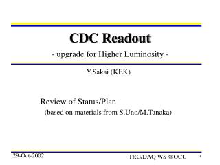
CDC. S. Uno KEK 2009.3.19. Endplate Design. sBelle. 350mm. 300mm. 250mm. Wire stringing. Strategy Vertically string wire Outer cylinder is assembled before wire stringing. We can access wires from inside of chamber. Nanae Taniguchi confirmed it with a hand-made mockup. 30°.

E N D
CDC S. Uno KEK 2009.3.19
Endplate Design sBelle 350mm 300mm 250mm
Wire stringing • Strategy • Vertically string wire • Outer cylinder is assembled before wire stringing. • We can access wires from inside of chamber. • Nanae Taniguchi confirmed it with a hand-made mockup. 30° f 500mm 173 mm 323 mm 12° 710 mm
Present status of Super-belle CDC front-end prototype. KEK Electronics group Y. Igarashi,K. Tauchi, M. Saito, M. Ikeno,M. Tanaka ,Y. Uchida and Takashi Taniguchi
CDC FE Prototype card Under 20cm • 16ch/board • BJT-ASB/Discriminator • FADC: over 20MHz / 10bit • FPGA : Vertex-5 LXT • TDC: 1 nsec counting • FADC reading • Control • FPGA: Spertan3A • SiTCP for CDC study • Connectors • RJ-45 for SiTCP • RJ-45 for DAQ timing signals • RJ-45 for DAQ data line • SFP for DAQ data line • Optical TX/RX for GDL • LEMO input x 3, output x1 • Shielded substrate RJ45 RJ45 ASB + Discriminator Optical Transceiver SFP Optical Transceiver FADC ASB + Discriminator FPGA (CONTROL, TDC) ASB + Discriminator FADC FPGA (SiTCP) ASB + Discriminator RJ45
Layout Preamplifier and discriminator(8ch/card) • The printed circuit board is in process and will be available in next month. FADC TDC using FPGA
TDC in FPGA ・Input ECL/LVDS/PECL16ch CLK、START/STOP ・Dynamic range 65us ・1ns/bit ・FIFO 1023hit/ch • TDC in FPGA with time resolution of 1nS. • Make the TDC circuit to a library. FPGA
TDC in FPGA Input: Hoshin 16bit TDC tester • 250MHz 4 phase Clock for 1 nsec resolution. Latch hit state and encode. RMS=0.51ns 0 0 1 1 4ns
AMP TEST with small tube chamber and 5.9 keV X-ray Nanae Taniguchi (KEK) Mar. 18
Amplifier • T-ASB • Used in trek/double beta experiment • After pulse • Cross talk • Hybrid ASB • Modify the T-ASB to be used super Belle-CDC
Setup • Small tube chamber (tungsten wire) • 5.9 keV X-ray • Gas(Ar90%+CH410%), P10 Gas Gas (Ar 90%+CH4 10%) Fe55 5.9keV X-ray ASB Tungsten wire Small tube chamber
Pulse shape • Same HV (1.65kV) • Signal from Hybrid ASB is attenuated (15dB), current Belle AMP (6dB) Current Belle T-ASB Hybrid ASB • Different shaping time • Over shoot disappeared (smaller). • Larger gain (~ x5)
Comparison of noise level Current Belle AMP T-ASB Hybrid ASB
After pulse T-ASB Hybrid ASB HV=1.7kV HV=1.7kV 400ns/div 200ns/div
Cross talk Ch 16 Ch 16 Ch 15 Ch 1 Ch 1 Ch 15 Cross talk is not so large.
Some discussion • Material of end plate (CFRP) • Gary’s proposal for readout electronics • We will discuss in next week. • Diameter of wire • Cluster counting method
CDC structure Shoji Uno (KEK) Dec-3rd, 2008
Baseline Design sBelle Belle
Wire Configuration Present CDC 250 mm 1200 mm New CDC 250 mm
Photo of small cell chamber Just after wire stringing Installation in 2003 summer
Curved Endplate • Deformation of endplate due to wire tension was calculated at design stage of present Belle CDC (Total tension: 3.5 Ton). Deformation(mm) 35.2 2.03 1.31 Present New
Weight • Endplate • Al, Thickness : 10mm (12mm) • 110kgx2 = 220kg (264kg) • Outer Cylinder • CRRP, Thickness : 5mm • 210kg • Electronics Board • G10, 48ch/board • 0.3kgx315 = 95kg
Calculation of deformation and etc • Deformation of Aluminum endplate • Thickness of endplate 10mm 12mm • Deformation 1/t3 1 0.58 • Tension of field wire 120g 80g • Gravitational sag, Sense : 120mm(80g), Field:300mm(80g) • Total tension 4.8ton • Stress calculation • Thickness of outer cylinderCFRP:mm • Transition structure between endplate and outer cylinder • Support structure • Structure for wiring jig • Simpler one as compared with Belle-CDC • Etc.
Wire stringing • Now, I am thinking a vertical stringing, not horizontal. • Once, I thought the horizontal stringing • Vertical stringing with outer cylinder. • Human can stand inside the chamber and can touch the wire. • Inner diameter without the small cell part : ~500mm • Inner diameter of present transition cylinder : 580mm • Stringing with tension can be done from outer layer. • Two-way method ( Belle-CDC ) is not necessary.
Installation • Removing and installation can be done using similar small bar in horizontal direction. Cathode installation in vertical direction CDC installation in horizontal direction
CLK For GFP LOGIC part diagram LVDS 2 pairs RocketIO GFP Optical connector LVDS 2 pairs RocketIO GFP SFP (Optical connector) CONTROL 3x4 16 ASB Discriminator TDC (with FIFO) TIMING LVDS 4x4 pairs RocketIO GFP LVDS 2 pairs RJ-45 LVDS 8 pairs FADC Ti ADS5287 5 FIFO LVDS 4 pairs RJ-45 16 De-serializer Spertan3A SiTCP CLK 50MHz ASB Discriminator 15 100base PHY RJ-45 LVDS CLKs 48 8 TEST PIN CONTROL 32 DIP-SW ASB Discriminator LVDS 8 pairs FADC Ti ADS5287 PUSH SW Vertex-5 LXT (XC5VLX50T, IO:360pin) 3 5 LEMO 4 LEMO LVDS CLKs LED ASB Discriminator 8 LEMO DIP-SW 16 LEMO TEST PIN 8 Sampling CLK 20~40 MHz CLK 125MHz CLK 42.33MHz DAC (Vth)
Front-end(preamp) • 7mm□. • 48pin. • ASB. • GainSW. • 1/t tail cancellation.
Front-end (for the system test) ASB Amp. Shaper Buffer 4ch/chip Peaking time ~40nsec Gain : -360mV/pC ~ -1400mV/pC (4 step variable) Disc. ASB D-out protection A-out Fe source
Hybrid preamp • Common emitter amp. • 3 stage amplification.