Download
1 / 1
10 likes | 112 Views
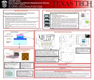
ANN NIRT GOALI Nano-Engineering Efficient Optoelectronic Devices NSF Grant ECS – 0609416 PIs: S. Nikishin, J. Berg, A. Bernussi, M. Holtz, H. Temkin Nano Tech Center, Texas Tech University, Lubbock TX-79409. (a). Basic LED Design. Starting surface (GaN). p -type AlGaN.

E N D
ANN NIRT GOALI Nano-Engineering Efficient Optoelectronic Devices NSF Grant ECS – 0609416 PIs: S. Nikishin, J. Berg, A. Bernussi, M. Holtz, H. Temkin Nano Tech Center, Texas Tech University, Lubbock TX-79409 (a) Basic LED Design Starting surface (GaN) p-type AlGaN AlN/AlGaN active region (b) E-beam lithography n-type AlGaN AlGaN or AlN template (c) Plasma etching a b d c Mask removal Nanophotonic Texturing Experiments for Enhancing Light Extraction – GaN • Basic process flow combines electron-beam lithography (SEM) and • plasma etching. • - Pore-to-pore pitch fixed at 1 μm. • - Pore diameter varied from 125 to 700 nm. • - Pore depth ~ 400 nm. • 2. SEM-cathodoluminescence intensity found to increase systematically • with pore area fraction. Increase is ~ double starting GaN layer. • A quantitative model is derived in which the net intensity is expressed • as the sum of intensities originating from the near-surface and • pore-bottom regions. The combined terms describe well the observed • dependence (not shown). • 3. SEM-cathodoluminescence peak red shifts with pore area fraction. • Shift interpreted based on relaxation of biaxial compressive stress. • Interpretation quantitatively confirmed by finite element simulation of • stress. Active Region Nano-Engineering The room temperature CL intensity Of QWs versus NH3 flux. Insets are depiction of quantum structure formation and TEM cross-section of a domain. Ammonia flux, growth mode, and corresponding RHEED images (insets a, b, c, and d) versus growth time of well material. Sample #1 (21 s growth time) – onset of 3D growth mode; #2 (26 s growth time) – at least 3/5 of well is grown in 3D mode; sample #3 (32 s growth time); sample #4 (42 s growth time) – onset of 3D →2D transition. 10.0 7.5 5.0 2.5 0.0 CL and PL data versus growth time of well material. PL excitation energy density is 0.72 µJ/cm2. (a) peak position, (b) intensity, and (c) 1/e decay time. The dashed horizontal line is the bandgap of the bulk Al0.4Ga0.6N material. Filled circle is CL of 2D grown well material. 0 2.5 5.0 7.5 10.0 • Motivation and Overview • Develop and apply methods of nanoengineering to improve light extraction properties of ultraviolet light-emitting diodes (LEDs). • The main efforts in year one were guided toward: • Nanoengineering of active region of UV LEDs using growth of AlGaN/AlGaN on AlGaN and AlN template substrates (GOALI partner – TDI Inc.) • Superlattices with AlGaN quantum dots in well material • Detailed characterization of these materials using X-ray diffraction, photoluminescence, micro-cathodoluminescence, atomic force microscopy, and transmission electron microscopy • Fabrication of nanophotonic surfaces on Si and GaN using nanolithography and plasma etching • Study of optical properties and light extraction efficiency of nano-structured GaN substrates Substrate design for improved epitaxy. (GOALI partner – TDI Inc.) Plan-view 10 X 10 μm2 AFM scan of HVPE grown 6.4 μm thick AlN/sapphire template. The surface RMS roughness is ~ 3 nm. Step-flow growth mode dominates. X-ray reciprocal space map (RSM) for (0002) reflection of AlN template. FWHMω-scan=100" & FWHM2Θ-ω=110". Inset: TEM cross-section of AlN/sapphire interface. Educational Impact This project provides nine students at the BS, MS, and PhD levels with a fully integrated multidisciplinary setting for research and training. Of the students involved in this work, five are female, and one of those was African-American. Three senior researchers are involved in research under this program. Collaborators Technologies and Devices International, Inc.; Army Research Laboratory; Veeco Instruments, Inc.; Soft-Impact, Ltd.; The Fox Group, Inc. Select publications under this grant “Transmission properties of nanoscale aperture arrays in metallic masks on optical fibers,” J. Appl. Phys. 101, 014303 (2007). “Selective area growth of GaN nano islands by metal organic chemical vapor deposition: experiments and computer simulations,” Proc. Mat. Res. Soc. Symp., 955, 0955-I07 (2007). “Enhanced luminescence from AlxGa1-xN/ AlyGa1-yN quantum wells grown by gas source molecular beam epitaxy with ammonia,” Proc. SPIE Photonics Conf., 6473, 647306 (2007). “X-ray diffraction study of AlN/AlGaN short period superlattices”, J. Appl. Phys., JR07-3866R (2007). “Deep UV light emitting diodes and solar blind photodetectors grown by gas source molecular beam epitaxy”, J. Mater. Sci: Mater Electron, DOI: 10.1007/s10854-007-9405-3 (2007). “Luminescence properties of AlxGa1-xN (0.4<x<0.5)/AlyGa1-yN (0.6<y≤1) quantum structures grown by gas source molecular beam epitaxy”, physica status solidi c (2007). “Influence of photonic nanotexture on the optical properties of GaN”, Appl. Phys. Lett. 91, 103115 (2007). 50-mm AlN free standing wafer fabricated at TDI Inc. HVPE growth of thick AlN layer on SiC substrates and subsequent removal of the SiC substrate by RIE. (Courtesy of TDI Inc.)