Download
1 / 37
440 likes | 950 Views
Project Work Nanoscience. X-Ray Diffraction Analysis of Ⅲ-Ⅴ Superlattices : Characterization, Simulation and Fitting. Xiangyu Wu Enlong Liu Mentor: Clement Merckling EPI Group @ imec. Outline. Introduction XRD Principle Superlattice Diffraction Results and Discussions

E N D
Project Work Nanoscience X-Ray Diffraction Analysis of Ⅲ-ⅤSuperlattices:Characterization, Simulation and Fitting Xiangyu Wu Enlong Liu Mentor: Clement Merckling EPI Group @ imec
Outline • Introduction • XRD • Principle • Superlattice Diffraction • Results and Discussions • Sample Structure • XRD Experiments Results • Curves Analysis and Simulation • Peaks Belonging • Theoretical Calculation • Simulation Results • Comparison with TEM Results • Conclusion
Outline • Introduction • XRD • Principle • Superlattice Diffraction • Results and Discussions • Sample Structure • XRD Experiments Results • Curves Analysis and Simulation • Peaks Belonging • Theoretical Calculation • Simulation Results • Comparison with TEM Results • Conclusion
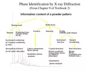
Introduction Superlattice (SL) is a periodic structure of layers of two (or more) materials. It can also refer to a lower-dimensional structure such as an array of quantum dots or quantum wires. Superlattice is linked to very advanced and complicated heterostructures. S.Y. Cheng, et al. Solid-State Electronics, 1999, 43(4):755-760. J.J.Gu, et al. IEDM12-529 http://en.wikipedia.org/wiki/Superlattice M. Cooke. Ⅲ-Ⅴs Review, 2006 19(6): 22-26 http://mbe.rcast.u-tokyo.ac.jp/index_eng.html
Introduction Epitaxy Vapor Phase Epitaxy (VPE) Molecular Beam Epitaxy(MBE) Slow growth rate • SL Growth Interfacial layer control • Characterization: Transmission Electron Microscopy (TEM) • Issue of TEM: • Only used to characterize small area on wafer; • Need sample preparation, very time-consuming; • Limit information, only thickness J.Warga, et al. Physica E, 2009, 41(6): 1040-3. Dark: Er-doped silicon-rich nitride; Bright: Si. X-Ray Diffraction
Outline • Introduction • XRD • Principle • Superlattice Diffraction • Results and Discussions • Sample Structure • XRD Experiments Results • Curves Analysis and Simulation • Peaks Belonging • Theoretical Calculation • Simulation Results • Comparison with TEM Results • Conclusion
XRD: Principle Bragg`s Law Two beams with identical wavelength and phase approach a crystalline solid and are scattered off two different atoms within it. The lower beam traverses an extra length of 2dsinθ. Constructive interference occurs when this length is equal to an integer multiple of the wavelength of the radiation. Bragg`s Law:
XRD: Principle s Detector X-ray tube w 2q • ω: Tune the angle between the emitter and substrate; • 2θ: Tune the angle between emitter and detector; • Ψ: Vertical rotation of substrate plane; • Φ: Horizontal rotation of the substrate plane; • x, y, z coordinate: move the substrate plane up, down, left, right, without rotation
XRD: Principle Rocking curve vsCoupled scan ω Si Omega axis sample detector 2θ Mono-chromator Analyzer ω detector detector Si Omega axis Si(Ge) sample Incident beam Mono-chromator 2θ=2ω+offset
Outline • Introduction • XRD • Principle • Superlattice Diffraction • Results and Discussions • Sample Structure • XRD Experiments Results • Curves Analysis and Simulation • Peaks Belonging • Theoretical Calculation • Simulation Results • Comparison with TEM Results • Conclusion
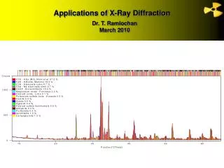
XRD: Superlattice Diffraction The greatest use of HRXRD in industry isthe characterization of epitaxial structures on compound semiconductors. The composition of ternaries, mismatch of quaternaries, mis-orientation, layer thickness, tilt, relaxation, indications of strain, curvature and stress, and area homogeneity have important influence on the performance of Ⅲ-Ⅴ and Ⅱ-Ⅵ semiconductors. MQW laser
XRD: Superlattice Diffraction The effect of substrate and epi-layer parameters upon the rocking curve
XRD: Superlattice Diffraction Lattice parameter and composition θ1 a2 d`hkl θ2 dhkl For zinc blende structure, a1 For (004) plane, Superlattice under full strain (e.g. InxGa1-xAs layer on InP substrate) Vegard’s Law:
XRD: Superlattice Diffraction XRD Superlattice period characterization θn By averaging over the positions of satellite peaks of order n, we got: n according Λ Λ where Λ is the thickness of a SL period, λCuKα1 =0.15405nm, is the nth-order peak of the MQW, is the zero-order peak. J.M. Vandenberg, A.T. Macrander, R.A. Hamm, M.B. Panish, Phys. Rev. B 44 (1991) 3991
Outline • Introduction • XRD • Principle • Superlattice Diffraction • Results and Discussions • Sample Structure • XRD Experiments Results • Curves Analysis and Simulation • Peaks Belonging • Theoretical Calculation • Simulation Results • Comparison with TEM Results • Conclusion
Results and Discussions Sample Structure (not to scale) S1: • InAlAs • Superlattice x5 • InP • InGaAs InxAl1-xAs InP InxGa1-xAs InP (001) InP (001) InP (001) • S2 • InAlAs • Superlatticex5 • InP: thickness ~x2 • InGaAs: thickness ~x2 S3 • InAlAs • Superlattice x5 • InGaAs: Same thickness as S2 • InAlAs: Unknown
Outline • Introduction • XRD • Principle • Superlattice Diffraction • Results and Discussions • Sample Structure • XRD Experiments Results • Curves Analysis and Simulation • Peaks Belonging • Theoretical Calculation • Simulation Results • Comparison with TEM Results • Conclusion
Results and Discussions XRD Experiments Results With offset From these curves ,we need to know: • Thickness of InAlAs buffer layerand the period of SL; • Compositionof each material.
Outline • Introduction • XRD • Principle • Superlattice Diffraction • Results and Discussions • Sample Structure • XRD Experiments Results • Curves Analysis and Simulation • Peaks Belonging • Theoretical Calculation • Simulation Results • Comparison with TEM Results • Conclusion
Results and Discussions Peaks belonging InAlAs 135nm InP 600μm Example to identify peaks from different sources.
Results and Discussions Peaks belonging Satellite peaks corresponds to superlattice period Inp Zero order peak gives information about mismatch(composition) InGaAs Inp InGaAs Inp InGaAs Inp InGaAs Inp InGaAs InP substrate
Results and Discussions Peaks belonging Repeat of SL period=N+2 N=3 Repeat=5 Inp InGaAs Inp InGaAs Inp InGaAs Inp InGaAs Inp InGaAs InP substrate
Results and Discussions Peaks belonging Inp InGaAs InAlAs 135nm Inp InGaAs InP 600μm Inp InGaAs Inp InGaAs Inp InGaAs InP substrate The total curve is the superposition of Layer and SL.
Results and Discussions Theoretical calculations Red arrow corresponds to fringes produced by InAlAs layer diffraction. InxAl1-xAs InP InxGa1-xAs Blue arrow corresponds to nth-order peak by diffraction of SL period InP (001)
Results and Discussions Theoretical calculations InxAl1-xAs For S2, the ideal thickness of SL is twice of that in S1. InP InxGa1-xAs According to previous data in S1, multiply by 2 directly. Coincidence Blue arrows refer to SL peaks, leading to average period 70 nm; Red arrows refer to Layer peaks, leading to average thickness 126 nm. InP (001)
Results and Discussions Theoretical calculations Arrows: peaks for Layer; Bracket: peaks for SL. InxAl1-xAs InP InxGa1-xAs Average Initial values for simulation All maximums remain in XRD, indicating that the thickness of two layers in SL are different. Only the total period can be calculated, which is 53.6nm. Besides, the thickness of InGaAs layer is the same as S2, we can take 34.0 nm as initial one ,which can also give that of InAlAs. InP (001)
Results and Discussions Simulation and fitting for S1 InxAl1-xAs InP InxGa1-xAs InP (001)
Results and Discussions Simulation and fitting for S2 InxAl1-xAs InP InxGa1-xAs InP (001)
Results and Discussions Simulation and fitting for S3 InxAl1-xAs InP InxGa1-xAs InP (001)
Results and Discussions Summary
Outline • Introduction • XRD • Principle • Superlattice Diffraction • Results and Discussions • Sample Structure • XRD Experiments Results • Curves Analysis and Simulation • Peaks Belonging • Theoretical Calculation • Simulation Results • Comparison with TEM Results • Conclusion
Comparisons with TEM Results InxAl1-xAs Layer Thickness S1 S2 S3 137 140 136 136nm 137nm 140nm
Comparisons with TEM Results SLs layers thickness InGaAs 16.0 18.5 InP S1 S2 S3 InGaAs 16.5 InP 18.0 InGaAs 16.0 18.5 InP 33 InGaAs InGaAs 30 16.0 InGaAs 38 InP InAlAs 21 18.5 InP InGaAs InGaAs 32 33 16.0 InGaAs InAlAs 20 38 InP InGaAs 32 InP 16.5 InGaAs 34 20 InAlAs InGaAs 32 InP 38 20 InAlAs 33 InGaAs InAlAs InGaAs 32 InP InAlAs 19 38 InGaAs 32 33 InGaAs 37 InP InAlAs 134 InGaAs33nm InP 38nm InGaAs32nm InAlAs 20nm InGaAs 16nm InP 18nm 20 nm 20 nm 20 nm 20 nm 20 nm InAlAs 136 InP InP 50 nm 50 nm 50 nm 50 nm 50 nm 50 nm 50 nm 50 nm 50 nm 50 nm
Comparisons with TEM Results Comparison
Outline • Introduction • XRD • Principle • Superlattice Diffraction • Results and Discussions • Sample Structure • XRD Experiments Results • Curves Analysis and Simulation • Peaks Belonging • Theoretical Calculation • Simulation Results • Comparison with TEM Results • Conclusion
Conclusion • XRD studies on superlattice samples with different compositions and periods. • Based on the information derived from XRD rocking curves, three models were established and simulated. • The fitting results of all three models not only gave information which TEM could not, but also corresponded well with data already given by TEM figures, indicating the reliability and accuracy of XRD measurement in superlattice structures. • With its non-destructive property and high efficiency in conducting experiments and results derivation, XRD will be a more suitable method for superlattice researches in many fields.
Thank you ! • Xiangyu Wu • Enlong Liu