Download
1 / 1
10 likes | 88 Views
100 m A. T lattice = 7.2K. 5 m A. T lattice = 2K. FIGURE 1. FIGURE 2. The authors gratefully acknowledge support for this project from NRC/British Council funding scheme, under contract no. 00CPR09. Hot Electron Energy Relaxation In AlGaN/GaN Heterostructures.

E N D
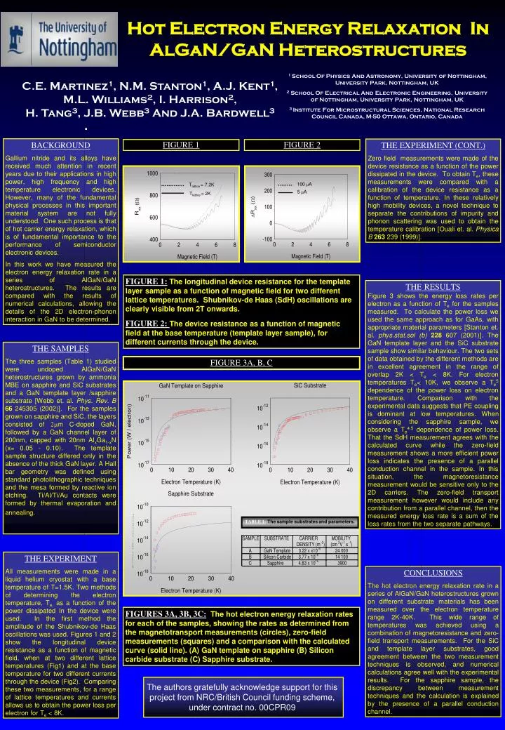
100 mA Tlattice = 7.2K 5 mA Tlattice = 2K FIGURE 1 FIGURE 2 The authors gratefully acknowledge support for this project from NRC/British Council funding scheme, under contract no. 00CPR09 Hot Electron Energy Relaxation In AlGaN/GaN Heterostructures 1 School Of Physics And Astronomy, University of Nottingham, University Park, Nottingham, UK 2 School Of Electrical And Electronic Engineering, University of Nottingham, University Park, Nottingham, UK 3 Institute For Microstructural Sciences, National Research Council Canada, M-50 Ottawa, Ontario, Canada C.E. Martinez1, N.M. Stanton1, A.J. Kent1, M.L. Williams2, I. Harrison2, H. Tang3, J.B. Webb3 And J.A. Bardwell3 BACKGROUND Gallium nitride and its alloys have received much attention in recent years due to their applications in high power, high frequency and high temperature electronic devices. However, many of the fundamental physical processes in this important material system are not fully understood. One such process is that of hot carrier energy relaxation, which is of fundamental importance to the performance of semiconductor electronic devices. In this work we have measured the electron energy relaxation rate in a series of AlGaN/GaN heterostructures. The results are compared with the results of numerical calculations, allowing the details of the 2D electron-phonon interaction in GaN to be determined. THE EXPERIMENT (CONT.) Zero field measurements were made of the device resistance as a function of the power dissipated in the device. To obtain Te, these measurements were compared with a calibration of the device resistance as a function of temperature. In these relatively high mobility devices, a novel technique to separate the contributions of impurity and phonon scattering was used to obtain the temperature calibration [Ouali et. al. Physica B263 239 (1999)]. FIGURE 1:The longitudinal device resistance for the template layer sample as a function of magnetic field for two different lattice temperatures. Shubnikov-de Haas (SdH) oscillations are clearly visible from 2T onwards. FIGURE 2: The device resistance as a function of magnetic field at the base temperature (template layer sample), for different currents through the device. THE RESULTS Figure 3 shows the energy loss rates per electron as a function of Te for the samples measured. To calculate the power loss we used the same approach as for GaAs, with appropriate material parameters [Stanton et. al. phys.stat.sol (b)228 607 (2001)]. The GaN template layer and the SiC substrate sample show similar behaviour. The two sets of data obtained by the different methods are in excellent agreement in the range of overlap 2K < Te < 8K. For electron temperatures Te< 10K, we observe a Te5 dependence of the power loss on electron temperature. Comparison with the experimental data suggests that PE coupling is dominant at low temperatures. When considering the sapphire sample, we observe a Te4.5 dependence of power loss. That the SdH measurement agrees with the calculated curve while the zero-field measurement shows a more efficient power loss indicates the presence of a parallel conduction channel in the sample. In this situation, the magnetoresistance measurement would be sensitive only to the 2D carriers. The zero-field transport measurement however would include any contribution from a parallel channel, then the measured energy loss rate is a sum of the loss rates from the two separate pathways. THE SAMPLES The three samples (Table 1) studied were undoped AlGaN/GaN heterostructures grown by ammonia MBE on sapphire and SiC substrates and a GaN template layer /sapphire substrate [Webb et. al. Phys. Rev. B66 245305 (2002)]. For the samples grown on sapphire and SiC, the layers consisted of 2mm C-doped GaN, followed by a GaN channel layer of 200nm, capped with 20nm AlxGa1-xN (x= 0.05 - 0.10). The template sample structure differed only in the absence of the thick GaN layer. A Hall bar geometry was defined using standard photolithographic techniques and the mesa formed by reactive ion etching. Ti/Al/Ti/Au contacts were formed by thermal evaporation and annealing. FIGURE 3A, B, C TABLE 1:The sample substrates and parameters. THE EXPERIMENT All measurements were made in a liquid helium cryostat with a base temperature of T=1.5K. Two methods of determining the electron temperature, Te, as a function of the power dissipated In the device were used. In the first method the amplitude of the Shubnikov-de Haas oscillations was used. Figures 1 and 2 show the longitudinal device resistance as a function of magnetic field, when at two different lattice temperatures (Fig1) and at the base temperature for two different currents through the device (Fig2). Comparing these two measurements, for a range of lattice temperatures and currents allows us to obtain the power loss per electron for Te < 8K. CONCLUSIONS The hot electron energy relaxation rate in a series of AlGaN/GaN heterostructures grown on different substrate materials has been measured over the electron temperature range 2K-40K. This wide range of temperatures was achieved using a combination of magnetoresistance and zero-field transport measurements. For the SiC and template layer substrates, good agreement between the two measurement techniques is observed, and numerical calculations agree well with the experimental results. For the sapphire sample, the discrepancy between measurement techniques and the calculation is explained by the presence of a parallel conduction channel. FIGURES 3A, 3B, 3C:The hot electron energy relaxation rates for each of the samples, showing the rates as determined from the magnetotransport measurements (circles), zero-field measurements (squares) and a comparison with the calculated curve (solid line). (A) GaN template on sapphire (B) Silicon carbide substrate (C) Sapphire substrate.