Download

1 / 23
230 likes | 384 Views
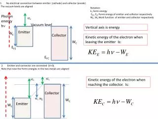
Common-Source (Emitter) Amplifiers with Resistive Loads. Dr. Paul Hasler. V dd. V dd = 5.0V. GND. Basic Resistive Load Circuits. R 1. R 1. V out. V out. V in. V in. GND. Common E / S: Resistive Load. V dd. V dd = 5.0V. GND. Common Source / Emitter. Output Voltage Bias = 3.0V.

E N D
Common-Source (Emitter) Amplifiers with Resistive Loads Dr. Paul Hasler
Vdd Vdd= 5.0V GND Basic Resistive Load Circuits R1 R1 Vout Vout Vin Vin GND
Vdd Vdd= 5.0V GND Common Source / Emitter Output Voltage Bias = 3.0V R1 R1 Vout Vout Vin Vin GND
Vdd Vdd= 5.0V GND What is the bias current? Iref = (2V) / R1 Common Source / Emitter Output Voltage Bias = 3.0V R1 R1 Vout Vout Vin Vin GND
Vdd Vdd= 5.0V GND Common Source / Emitter Output Voltage Bias = 3.0V R1 R1 Iref = (2V) / R1 Vout Vout Vin Vin GND
Vdd Vdd= 5.0V GND Common Source / Emitter Output Voltage Bias = 3.0V R1 R1 Iref = (2V) / R1 Vout Vout Vin Vin GND BJT / Subthreshold VT (2V) / R1 = Ico eVin/UT
Vdd Vdd= 5.0V GND Common Source / Emitter Output Voltage Bias = 3.0V R1 R1 Iref = (2V) / R1 Vout Vout Vin Vin GND BJT / Subthreshold VT (2V) / R1 = Ico eVin/UT Vin = UT ln ( (2V) / R1 Ico )
Vdd Vdd= 5.0V GND Common Source / Emitter Output Voltage Bias = 3.0V R1 R1 Iref = (2V) / R1 Vout Vout Vin Vin GND BJT / Subthreshold VT Above Threshold (Vd > Vg - VT ) (2V) / R1 = Ico eVin/UT Vin = UT ln ( (2V) / R1 Ico )
Vdd Vdd= 5.0V GND Common Source / Emitter Output Voltage Bias = 3.0V R1 R1 Iref = (2V) / R1 Vout Vout Vin Vin GND BJT / Subthreshold VT Above Threshold (Vd > Vg - VT ) (2V) / R1 = (K/2) (Vin - VT )2 (2V) / R1 = Ico eVin/UT Vin = VT + sqrt( (4V) / (K R1) ) Vin = UT ln ( (2V) / R1 Ico )
Vdd Vdd= 5.0V GND Common Source / Emitter Output Voltage Bias = 3.0V R1 R1 Iref = (2V) / R1 Vout Vout Have bias Vin Vin Vin GND
V3 + V - V1 rp gmV ro V2 V2 Small-Signal Modeling V3 V3 I I V1 V1 V2 V2 rp gm ro Av BJT (UTb) / I I / UT VA / I VA / UT Above VT MOSFET 2I /(V1-V2 -VT) VA / I 2VA/(V1-V2 -VT) Sub VT MOSFET kI / UT VA / I kVA / UT
Vdd Vdd= 5.0V GND Small-Signal Model Output Voltage Bias = 3.0V R1 R1 Iref = (2V) / R1 Vout Vout Have bias Vin Vin Vin GND Compute Transconductance (gm)
Vdd Vdd= 5.0V GND Small-Signal Model Output Voltage Bias = 3.0V R1 R1 Iref = (2V) / R1 Vout Vout Have bias Vin Vin Vin GND Compute Transconductance (gm) BJT / Subthreshold VT gm = I / UT = (2V) / (R1 UT)
Vdd Vdd= 5.0V GND Small-Signal Model Output Voltage Bias = 3.0V R1 R1 Iref = (2V) / R1 Vout Vout Have bias Vin Vin Vin GND Compute Transconductance (gm) BJT / Subthreshold VT Above Threshold (Vd > Vg - VT ) gm = 2I /(Vin -VT) = (4V) / (R1 (Vin -VT) ) gm = I / UT = (2V) / (R1 UT)
Vdd Vdd= 5.0V GND Small-Signal Model Output Voltage Bias = 3.0V Iref = (2V) / R1 R1 R1 Have bias Vin Vout Vout gm = (2V) / (R1 UT) Vin Vin or GND gm = (4V) / (R1 (Vin -VT) )
Vdd Vdd= 5.0V GND GND Vin Vout + V - gmV R1 rp Small-Signal Model Output Voltage Bias = 3.0V Iref = (2V) / R1 R1 R1 Have bias Vin Vout Vout gm = (2V) / (R1 UT) Vin Vin or GND gm = (4V) / (R1 (Vin -VT) )
Vdd Vdd= 5.0V GND GND Vin Vout + V - gmV R1 rp Small-Signal Model Output Voltage Bias = 3.0V Iref = (2V) / R1 R1 R1 Have bias Vin Vout Vout gm = (2V) / (R1 UT) Vin Vin or GND gm = (4V) / (R1 (Vin -VT) ) Gain = - gmR1 = - [ (2V) /(R1UT) ] R1 = - (2V) /UT
Vdd Vdd= 5.0V GND GND Vin Vout + V - gmV R1 rp Small-Signal Model Output Voltage Bias = 3.0V Iref = (2V) / R1 R1 R1 Have bias Vin Vout Vout gm = (2V) / (R1 UT) Vin Vin or GND gm = (4V) / (R1 (Vin -VT) ) Gain = - gmR1 = - [ (2V) /(R1UT) ] R1 = - (2V) /UT or Gain = -(4V) / (Vin -VT)
Vdd Vdd= 5.0V GND GND Small-Signal Model Output Voltage Bias = 3.0V Iref = (2V) / R1 R1 R1 Have bias Vin Vout Vout gm = (2V) / (R1 UT) Vin Vin or GND gm = (4V) / (R1 (Vin -VT) ) Vout Vin + V - gmV R1 rp ro
Vdd Vdd= 5.0V GND GND Small-Signal Model Output Voltage Bias = 3.0V Iref = (2V) / R1 R1 R1 Have bias Vin Vout Vout gm = (2V) / (R1 UT) Vin Vin or GND gm = (4V) / (R1 (Vin -VT) ) Vout Vin Gain = - [(2V) / UT ][1 + (2V)/ VA ] + V - or gmV R1 rp ro Gain = -[(4V)/(Vin -VT)][1 + (2V)/ VA ]
Vdd Vdd= 5.0V GND GND Vin Vout + V - gmV R1 rp Small-Signal Model Output Voltage Bias = 3.0V Iref = (2V) / R1 R1 R1 Have bias Vin Vout Vout gm = (2V) / (R1 UT) Vin Vin or GND gm = (4V) / (R1 (Vin -VT) ) Gain = - (2V) /UT or Gain = -(4V) / (Vin -VT)
Vdd Vdd= 5.0V GND GND Vin Vout + V - gmV R1 rp Small-Signal Model Output Voltage Bias = 3.0V Iref = (2V) / R1 R1 R1 Have bias Vin Vout Vout gm = (2V) / (R1 UT) Vin Vin or GND gm = (4V) / (R1 (Vin -VT) ) Gain = - (2V) /UT or Gain = -(4V) / (Vin -VT) Output Resistance = R1