Download
1 / 23
230 likes | 364 Views
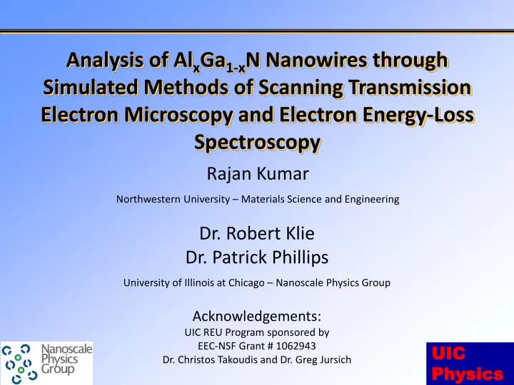
Analysis of Al x Ga 1-x N Nanowires through Simulated Methods of Scanning Transmission Electron Microscopy and Electron Energy-Loss Spectroscopy. Rajan Kumar Northwestern University – Materials Science and Engineering. Dr. Robert Klie Dr. Patrick Phillips

E N D
Analysis of AlxGa1-xN Nanowires through Simulated Methods of Scanning Transmission Electron Microscopy and Electron Energy-Loss Spectroscopy Rajan Kumar Northwestern University – Materials Science and Engineering Dr. Robert Klie Dr. Patrick Phillips University of Illinois at Chicago – Nanoscale Physics Group Acknowledgements: UIC REU Program sponsored by EEC-NSF Grant # 1062943 Dr. Christos Takoudis and Dr. Greg Jursich
Project Goals • Simulate nanowire images to better understand atomic composition of nanowires • Run Kirkland code, look for resolution changes in all three elements • Simulate EELS to better understand electrical properties of nanowires • - Run multiple scattering code, look for energy peaks • and their shape relative to composition • By characterizing the nanowire structure qualitatively, we can improve its properties to maximize efficiency for ultraviolet emission
Graded AlxGa1-xN Nanowires • New type of pn-junction not based on impurity doping, • but on grading composition from x = 0 to x = 1 • UV LED Applications • Need for atomic-scale characterization S.D. Carnevaleet al., Nano Letters, Vol. 10, 1-3, 2012
Scanning Transmission Electron Microscopy (STEM) • Incident electrons converge on specimen • Electrons scatter through specimen, contribute to image formation • Two types of detection • High Angle Annular Dark Field (HAADF) and Annular Bright Field (ABF) • HAADF good for Z contrast • ABF good for low weight elements E.J. Kirkland: ‘Advanced computing in electron microscopy’, 2ndedn, 11; 2010, New York, Springer
Scanning Transmission Electron Microscopy (STEM) • Incident electrons converge on specimen • Electrons scatter through specimen, contribute to image formation • Two types of detection • High Angle Annular Dark Field (HAADF) and Annular Bright Field (ABF) • HAADF good for Z contrast • ABF good for low weight elements • JEOL JEM-ARM 200CF • Down to 65 pm spatial resolution
STEM Images HAADF Image ABF Image
Imaging Simulation - Kirkland • Predict what a STEM image will look like for a given structure and imaging parameters • Kirkland code takes a continuous material and sections it into discrete slices • - Each slice is one layer of atoms separated by empty space E.J. Kirkland: ‘Advanced computing in electron microscopy’, 2ndedn, 142-143; 2010, New York, Springer
Electron Energy-Loss Spectroscopy (EELS) • Analyzing energy distribution of emitted electrons after interacting with a specimen • Two types of interactions: elastic and inelastic • These interactions cause the emitted electrons to lose a characteristic amount energy relative to the specimen it travels through R.F. Egerton: ‘EELS in the Electron Microscope’, 3rdedn, 6-21; 2011, New York, Springer
Spectra Simulation - FEFF9 Coherent superposition of standing waves Feff9 calculations vs experiment for O K-edge in SrTiO3 FEFF9 is a real space multiple scattering code for electronic structure, x-ray spectra, and EELS. Non-periodic structures (e.g. nanowires, surfaces) can be modeled efficiently. J. J. Rehr & R.C. Albers, Review of Modern Physics, Vol. 72, 624, 2000
Simulated Images - Pure GaN GaNHAADF GaN ABF
Simulated Images - Pure AlN AlNHAADF AlN ABF
Simulated Images - Single Graded Viewing Direction GaN rich GaN AlN rich Graded HAADF AlN AlN rich GaN rich Graded ABF
Simulated Images - Double Graded AlN GaN AlN rich AlN rich GaN rich GaN rich Graded HAADF Graded ABF
Comparison to STEM Images AlN rich GaN rich
Comparison to EELS Spectra GaN rich AlN rich
Comparison to EELS Spectra V. J. Keastet al., Journal of Microscopy, Vol. 203, 170, 2001
Summary • Simulated STEM (Kirkland code) • Higher nitrogen contrast in aluminum rich regions vs gallium rich regions • Gallium sites have higher intensities • Simulated EELS (FEFF9) • Confirmed three dominant peaks in AlN • More testing needed for GaN to determine why there is a secondary peak
Summary • Future Work • Graded FEFF9 calculations • Experiment with FEFF9 parameters • Collect more STEM images and EELS data to compare with simulations • Confirmed experimental image contrast comes from chemical ordering • This will help complete structural characterization of nanowires to verify their target growth
Microscopy – UIC’s JEOL JEM-ARM 200CF • Cold field emission (0.4 eV resolution) • Probe spherical aberration corrector (less than 78 pm spatial resolution) • GatanEnfina 1000 EELS system • HAADF, LAADF, BF/ABF detectors • Stages: • DT, ST, tomography • in situ: heating, cooling, liquid, STM
FEFF9 Calculations • Pure Crystals – GaN and AlN • Graded Crystal – change nearest neighbor sites