Download
1 / 12
120 likes | 213 Views
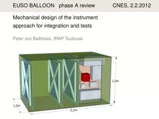
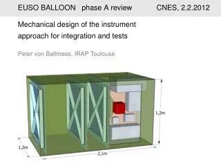
EUSO BALLOON EC-ASIC Electrical Interface. S. Ahmad , P. Barrillon, S. Blin, S. Dagoret, F. Dulucq, C. de La Taille, G. Martin-Chassard IN2P3-OMEGA LAL Orsay, France. Reminder of EC-ASIC. 6 ASICs, on top & bottom of the PCB 6 connectors (68 pins) ⇒ MAPMTs

E N D
EUSO BALLOONEC-ASIC Electrical Interface S. Ahmad, P. Barrillon, S. Blin, S. Dagoret, F. Dulucq, C. de La Taille, G. Martin-Chassard IN2P3-OMEGA LAL Orsay, France
Reminder of EC-ASIC • 6 ASICs, on top & bottom of the PCB • 6 connectors (68 pins) ⇒ MAPMTs • 1 connector (120 pins) ⇒ PDM Board 120 pins ASIC A ASIC B ASIC C ASIC D ASIC E ASIC F A B C D E F 68 pins 68 pins 68 pins 68 pins 68 pins 68 pins
EC-ASIC Interfaces Connections EC-ASIC ⇔ PDM: • Connector 120 pins should be enough • Choice: HIROSE FX2-120P-1.27DS • Header • Dimension=82mm x 7.5mm • Right angle type • Through hole
EC-ASIC Interfaces ① ASIC Parameters setting : Slow Control (SC) Registers • Daisy chain – 6 ASICs • Optional : Signal Monitoring(probe) – interface sharing • Serial TTL signals ② Data Transmission (I/O of Digital Module) • LVDS : • Readout Clock - 40 MHz • GTU - 400kHz, 98% Duty Cycle, Syncronised to ↓Readout Clock • Serial TTL: • Transmission On - Flag the Data Transmission to PDM • Data Out – Serial links for Data • Reset ③ Analog I/O: • LVDS : Fast ASIC Masking • TTL: • OR_FSU(6x) • OR_PA, OR_VFS & OR_KI – Not Used
SPACIROC Slow Control Slow Control - 1 Bit Cell • Features: • Shift registers • Non destructive readout • Radiation hardened • Data majority voter • Error detection • Low frequency operations • Components: • Scan Type DFF • Triple Data Latch • Majority & Error logic SPACIROC SC : 898 bits
EC-ASIC Slow Control 6 ASICs Daisy Chain : ASIC F ASIC A ASIC B Asr_in FSr_out Sr_rstb Sr_rstb Sr_rstb Sr_ck Sr_ck Sr_ck Load_sc Load_sc Load_sc Select_ din Select_ din Select_ din Select_ sc_probe Select_ sc_probe Select_ sc_probe SPACIROC ASIC SC : 898 bits EC-ASIC SC: 5 388 bits PDM SC : 32 328 bits
EC-ASIC Data Transmission • Data Transmission : • Starts after detecting of the rising edge ↑GTU • TransmitOn active for flagging the transmission • DataOut: StartBit=‘1’ • DataOut: MSB first, Ch0 to Ch7 (+Ch8 for KI) • Transmission ends with parity bit: • ‘1’ for even and ’0’ for odd number of 1s. • Total DataOut: • StartBit(1 bit) + Data(64 bits) + Parity(1 bit) • Data rate: 3.4 kbit/GTU *Full timing diagram available
Progress status • Slow Control Interface(PDM): • Heritage UFFO: Same ASIC and SC bit counts • Changes on EC: 4xASIC ⇒ 6xASIC • Full ASIC parameter settings & Readout • Data Readout Interface(PDM): • Heritage UFFO: Identical readout interface • Changes on EC: 4xASIC ⇒ 6xASIC • Readout Clock : 20MHz ⇒ 40MHz • Pinlist is pending the completion of EC-ASIC schematic • Possible rising problems: • Limitations on the ASIC DataOut buffer: max load ~20pF @40MHz • Short Cable length is preferred(max ~15cm) • Drawbacks on Multidrop LVDS ? (6 Loads) • Signal integrity (Crosstalk,…)
Digital Module Timing Diagram • GTU : 2% duty cycle synchronised on falling edge of ClkReadout • Global Reset (Rstb) at least 25 ns. 10
ASIC Interface IO signals for the ASIC communication: • Inputs (non exhaustive list) • 64 MAPMT anodes inputs + 1 dynode input • in<0…63>, last_dynode • Slow Control signals: • sr_in, select_din, sr_stb, sr_ck, load_sc (TTL) • Probe (analog/digital) signals: • sr_in, sr_clk, sr_rstb (TTL) • select_sc_prob (Shared I/O: sr_rstb, sr_ck, sr_in, sr_out) (TTL) • resetb : Digital Global Reset (TTL) • Val_evt (LVDS) : Trigger enable • GTU (LVDS) : 400kHz clock • ClockReadOut (LVDS) : 40MHz clock • VHi: defined voltage for digital high level outputs (1.5V) • VLo: defined voltage for digital low level outputs (0V) • trig_ext(TTL) : External Trigger for debugging Analog inputs FPGA Clocks from FPGA
ASIC Interface IO signals for the ASIC communication: • Outputs (non exhaustive list) • Data Output • transmit_on (VHi-VLo) • Data Out (VHi-VLo) : data_pc<0…7>, data_ki • Or trigger outputs(VHi-VLo) : • OR_trig_fsu,OR_trig_pa,OR_trig_vfs : PC • OR_ki_sum,OR_ki_dynode : KI • Probes : Analog & Digital • Probes/Slow Control output: • sr_out (Shared), error_sc (Slow Control) • Various current and voltage monitoring (Bias, Threshold, etc..)