Download
1 / 32
320 likes | 396 Views
MicroJava-701. Philipp Baecker · Johannes Bungert · Andreas Gladisch · Christian Titze. Introduction. The first microprocessor that executes Java bytecodes directly in hardware Some results suggest that MicroJava 701 will be twice as fast as a 266 MHz Pentium II system on Java code

E N D
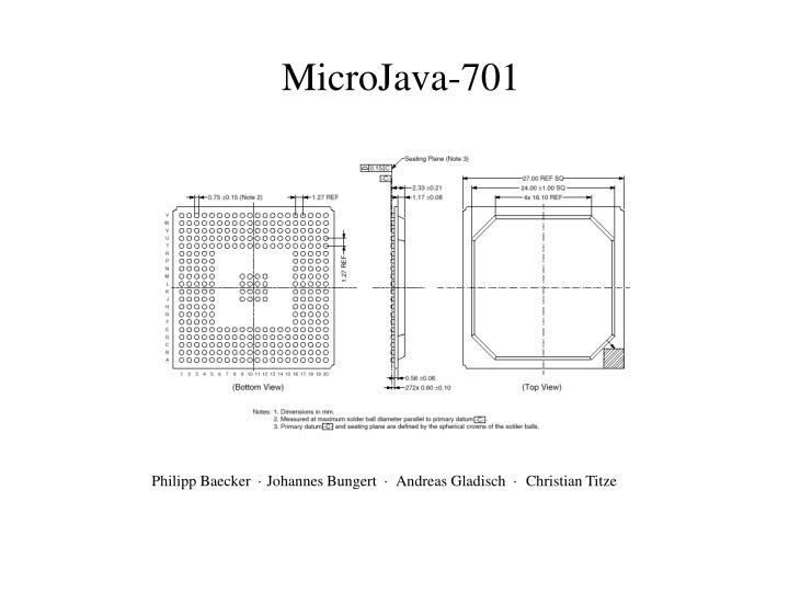
MicroJava-701 Philipp Baecker · Johannes Bungert · Andreas Gladisch · Christian Titze
Introduction • The first microprocessor that executes Java bytecodes directly in hardware • Some results suggest that MicroJava 701 will be twice as fast as a 266 MHz Pentium II system on Java code • MicroJava 701 looks to be a dynamite bargain for customers determined to build Java-execution machines. • What kind of machines might those be? • The hypothetical Java-based network computer has been slow to appear, perhaps because Java applications are not thick on the ground.
Introduction • Without plentiful Java apps, Java systems are superfluous, without the Java-system, the apps may not come. • The 701 looks better the more bytecode the system has to run. • For an all bytecode-system, the 701 is probably faster and cheaper than anything else. • MicroJava 701 makes sense for some small fraction of the market (that does not now exist) that mainly relies on Java code and does not already have a microprocessor in it.
Introduction • Java hardware, software, education, and advertising are sun’s featured products. • Sun is more interested in Java itself than in Java chips specifically. • So, Java chips are a complement, not a replacement for software only Java environments.
Features • picoJava-II Performance Java architecture • Operating Frequency of 133 to 200 MHz • Maximum Power Consumption of 4 W • 0.25 micron CMOS technology. • 64 × 32-bit Stack Cache • 16 Kbyte direct-mapped Instruction cache • 16 Kbyte, two-way set-associative Data cache • 32-bit Integrated Floating-Point Unit • Support for big- and little-endian data byte ordering • Interface to PCI Bus
Features • Integrated memory controller • Programmable I/O • Ten External Interrupts • Power management • Local Bus for low cost peripheral expansion, connection to 8-bit, 16-bit, or 32-bit slave devices (e. g. a boot PROM) • Interrupt Controller and multiple timers (programmability of interrupt priorities). • 2.5 V for the CPU core and 3.3 V for I/O
Memory Map • The microJava-701 CPU permits the following memory regions to be placed anywhere within the CPU’s 1 GB of addressable address space: • DRAM (both EDO and SDRAM)—four banks • Local Bus—four banks • PCI Memory/IO—three banks • The fixed regions in the memory map are as follows: • Registers • Boot code selected by FLASH_CS#—only the starting address is fixed (the Region’s size can be programmed)
Integer Unit (IU) • Java integer instructions • defined in the Java Virtual Machine Specification • extended picoJava-II specific instructions • 64-word (32-bit) stack cache • Executes prefetched instructions using a six-stage pipeline • Supports instructions such as shift, integer multiply, integer divide and stack manipulation. • Little-endian and big-endian data representation. • Up to four instructions can be folded together and executed in parallel.
Floating Point Unit (FPU) • The FPU executes all single-precision and double-precision floating-point instructions as defined in the Java • Virtual Machine Specification. • Has its own • microcode sequencer • Floating point adder • Floating-point multiplier/divider. • float and double represent single-precision 32-bit and double-precision 64- bit format IEEE 754 values as specified in IEEE Standard for Binary Floating-Point Arithmetic
Floating Point Unit (FPU) • float and double • Positive and negative sign-magnitude numbers • Positive and negative zeroes • Positive and negative infinities • Special Not-a-Number (NaN) value • Finite nonzero values of type float: s xfa m xfa 2e, where • s is +1 or –1, • m is a positive integer less than 224, • e is an integer between –149 and 104, • Smallest positive nonzero value:1.40239846e–45F • Largest positive nonzero value: 3.40282347e+38F
Floating Point Unit (FPU) • Finite nonzero values of type float: s xfa m xfa 2e, where • s is +1 or 1, • m is a positive integer less than 224, • e is an integer between 149 and 104, • Smallest positive nonzero value:4.94065645841246544e– 324 • Largest positive nonzero value: 1.79769313486231570e+308 • Floating-point values are ordered • NaN is unordered
Cache • Instruction Cache • 16kByte in size • Direct mapped cache organized as 1024 lines × 16Byte. • Instruction cache line fill done four 32-bit words at a time. • Data Cache • 16kByte in size. • Each set is 512 lines × 16Byte. • Data cache line fill done four 32-bit words at a time.
DRAM Memory Interface • Complete EDO DRAM and SDRAM controller generates all signals necessary to support from 1 MByte to 256 MBytes of EDO DRAM or SDRAM. • EDO DRAM at speeds of 70ns, 60ns, and 50ns. • SDRAM at frequencies of either 1/2, 1/3, or 1/4 the CPU clock rate (e.g., at 100 MHz, 66 MHz, or 50 MHz for a 200 MHz CPU). • DRAM devices must be of the same technology and speed grade. • 32-bit and 64-bit DRAM devices • DRAM system is organized as four banks, varying from 4 MBytes to 64 MBytes in size.
Flash Memory Interface • Local bus interface suitable for attaching • Flash memory boot PROM • Super I/O controller • Other slave I/O devices with timings similar to Flash memory. • Five banks provided for local bus connections • One bank dedicated for Flash memory that has a fixed starting address 0 to be used for the boot program. • 64KByte to 1GByte of Flash memory. • Data bus width of 8-bit, 16-bit or 32-bit
Interrupt Controller • 15 interrupt levels and one nonmaskable interrupt (NMI) • NMI, six external interrupts, EXT_INTR[5:0], and four low level interrupts, LL_INTR#[3:0] made available for general purpose use. • Four sources of internally generated interrupts: • tick timer, • general purpose timer, • watchdog timer • PCI error. • Two software interrupts. • An interrupt source can be mapped to any of 15 levels.
Interrupt Controller • Level-triggered interrupts triggered with a low logic level • Edge-triggered interrupts triggered on rising edges. • Edge-triggered interrupts cleared by writing a one to the bit position in the Pending Register (PEND_INT) to be cleared. • After an edge-triggered interrupt has been pro-cessed, its pending bit must be cleared before another trigger event can be sensed. • Trigger type of external interrupts, EXT_INTR[5:0], are programmable, while low level trigger interrupts, LL_INTR#[3:0], are always triggered with a low level and are normally used for PCI bus interrupts.
DRAM Bank Aliasing BER: Bank Enable Register DADR: DRAM Access Decode Register DADAR: DRAM Access Decode Alias Register
Missing Handbook? • Programmer’s Reference Manual picoJava-II processor core will not be available before 1999 • But: microJava-701 is hardware implementation of JVM (Java Virtual Machine) plus extensions (absolute addressing!) • JVM instruction set uses opcodes and mnemonics also used by the silicone chip
Instruction Set • Instructions identified by one-byte opcode • More complex operations have to be emulated • Example of the inner loop of the Virtual Machine:do { fetch an opcode; if (operands) fetch operands; execute the action for the opcode;} while (there is more to do);
Load and Store Instructions • Load and store instructions transfer values between the Virtual Machine’s local variables and operand stack:iload, iload_<n>, lload, lload_<n>fload, fload_<n>, dload, dload_<n>aload, aload_<n>
Arithmetic Instructions • Two types: • integer value processing • floating point value processing • No support of byte, short, and char types
Arithmetic Instruction Set • Add: iadd, ladd, fadd, dadd. • Subtract: isub, lsub, fsub, dsub. • Multiply: imul, lmul, fmul, dmul. • Divide: idiv, ldiv, fdiv, ddiv. • Remainder: irem, lrem, frem, drem. • Negate: ineg, lneg, fneg, dneg. • Shift: ishl, ishr, iushr, lshl, lshr, lushr. • Bitwise OR: ior, lor. • Bitwise AND: iand, land. • Bitwise exclusive OR: ixor, lxor. • Local variable increment: iinc.
Type Conversion Instructions • Support: • int to long, float, or double • long to float or double • float to double
Instruction Set Example • Instruction: swap • Operation: Swap top two operand stack words • Forms: swap = 95 (0x5f) • Stack: … , word2, word1 > …, word1, word2 • Description: The top two words on the operand stack are swapped
Perfomance and Speed • 85% of Java Bytecode processed in hardware • Frequently occurring Sequences replaced • Innovative Hardware Stack • Accelerated Stack Management
Innovative Hardware Stack • Top 64 entries on the stack contained within picoJava on-chip stack cache • Java programs invoke methods • Streamlining method invocation substantially improves the performance of Java code • Overlap between the methods allows direct parameter passing without copying
Accelerated Stack Management • Access usually limited to the top portion of the stack • Random, single-cycle access to the stack: FOLDING • moving data to top variable and consuming that data “folded” into one operation.