Download
1 / 1
10 likes | 101 Views
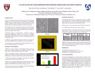
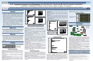
CNMS User Program Highlight. Topographic and Spectroscopic Characterization of Electronic Edge States in CVD Grown Graphene Nanoribbons Minghu Pan, 1 E. Costa Girão, 2,7,8 Xiaoting Jia, 4 Sreekar Bhaviripudi, 4 Qing Li, 1 Jing Kong, 5 V . Meunier, 2,3 and Mildred S. Dresselhaus 5,6

E N D
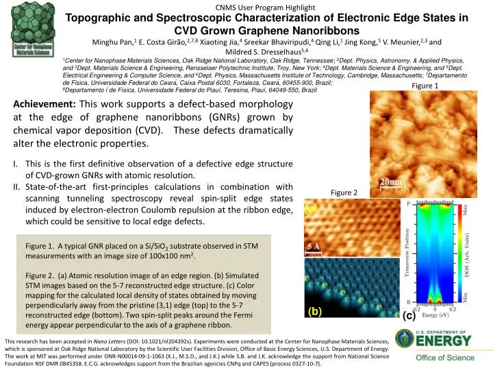
CNMS User Program Highlight Topographic and Spectroscopic Characterization of Electronic Edge States in CVD Grown Graphene Nanoribbons Minghu Pan,1E. Costa Girão,2,7,8Xiaoting Jia,4Sreekar Bhaviripudi,4Qing Li,1Jing Kong,5V. Meunier,2,3and Mildred S. Dresselhaus5,6 1Center for Nanophase Materials Sciences, Oak Ridge National Laboratory, Oak Ridge, Tennessee; 2Dept. Physics, Astronomy, & Applied Physics, and 3Dept. Materials Science & Engineering, Rensselaer Polytechnic Institute, Troy, New York; 4Dept. Materials Science & Engineering, and 5Dept. Electrical Engineering & Computer Science, and 6Dept. Physics, Massachusetts Institute of Technology, Cambridge, Massachusetts; 7Departamento de Fisica, Universidade Federal do Ceará, Caixa Postal 6030, Fortaleza, Ceará, 60455-900, Brazil;8Departamento í de Física, Universidade Federal do Piauí, Teresina, Piauí, 64049-550, Brazil Figure 1 • Achievement: This work supports a defect-based morphology at the edge of graphenenanoribbons (GNRs) grown by chemical vapor deposition (CVD). These defects dramatically alter the electronic properties. • This is the first definitive observation of a defective edge structure of CVD-grown GNRs with atomic resolution. • State-of-the-art first-principles calculations in combination with scanning tunneling spectroscopy reveal spin-split edge states induced by electron-electron Coulomb repulsion at the ribbon edge, which could be sensitive to local edge defects. Figure 2 (a) Figure 1. A typical GNR placed on a Si/SiO2 substrate observed in STM measurements with an image size of 100x100 nm2. Figure 2. (a) Atomic resolution image of an edge region. (b) Simulated STM images based on the 5-7 reconstructed edge structure. (c) Color mapping for the calculated local density of states obtained by moving perpendicularly away from the pristine (3,1) edge (top) to the 5-7 reconstructed edge (bottom). Two spin-split peaks around the Fermi energy appear perpendicular to the axis of a graphene ribbon. (b) (c) This research has been accepted in Nano Letters (DOI: 10.1021/nl204392s). Experiments were conducted at the Center for Nanophase Materials Sciences, which is sponsored at Oak Ridge National Laboratory by the Scientific User Facilities Division, Office of Basic Energy Sciences, U.S. Department of Energy. The work at MIT was performed under ONR-N00014-09-1-1063 (X.J., M.S.D., and J.K.) while S.B. and J.K. acknowledge the support from National Science Foundation NSF DMR 0845358. E.C.G. acknowledges support from the Brazilian agencies CNPq and CAPES (process 0327-10-7).