Download
1 / 33
330 likes | 472 Views
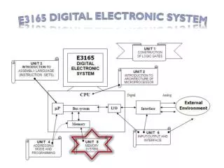
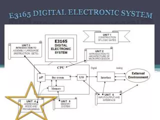
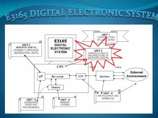
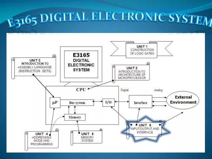
E3165 DIGITAL ELECTRONIC SYSTEM. INTRODUCTION. Microprocessor must communicate (read and write) with RAM, ROM or I/O devices. To ensure the microprocessor can communicate smoothly, we need interfacing. Operation of input/output: Unconditional I/O Transfer – MPU Initiated Interrupt System

E N D
INTRODUCTION • Microprocessor must communicate (read and write) with RAM, ROM or I/O devices. • To ensure the microprocessor can communicate smoothly, we need interfacing. • Operation of input/output: • Unconditional I/O Transfer – MPU Initiated • Interrupt System • Direct Memory Access • Hand-shaking
UNCONDITIONAL I/O TRANSFER • Unconditional transfer - Used only in situation where an output device is always ready to accept data from the MPU or an input device always has data ready for the MPU. Therefore no need for any exchange of control signals. • Conditional transfer – MPU will send / receive data when the output device ready. Need some control signals.
INTERRUPT SYSTEM • Interrupt is a signal that causes the microprocessor to end its normal execution to initiate interrupt operation. • 2 types: • Hardware – occur when microprocessor interrupt pin given truth logic. (Figure 2.6, Unit 2/18) • Software – using instruction programming.
HOW INTERRUPT INITIATED • Microprocessor receive interrupt request signal. Existing process will proceed until end before entertain the interrupt request. • PC and register value will be stored (push) into stack. • PC will be load with address of interrupt sequence (interrupt service routine/ISR). • After executing the interrupt sequence(ISR), data in stack will be loaded back (pull) from stack to PC and register respectively. • Microprocessor will continue the original program.
INTERRUPT SYSTEM • Types of interrupt: • Maskable Interrupt • Interrupt signals that can be received or not by microprocessor, depends on priority. • Nonmaskable Interrupt • Interrupt signal that must be received by the microprocessor. • The interrupt advantage • To ensure the I/O devices or peripheral devices interrupting microprocessor to initiate. • Reduce time and cost in such a way that interrupt only occurs when microprocessor receive an interrupt signal.
DIRECT MEMORY ACCESS (DMA) • DMA helps microprocessor in data transfer between memory and I/O. So microprocessor cando other work. • Example: 8085A with pin HOLD and HLDA. 8257 DMA controller as in Figure 6.2 • DMA give high input to the 8085A through pin HOLD. • 8085A will complete the execution of current process. • 8085A will puts the buses to Hi-Z and send high input to DMA through pin HLDA. • DMA take over the buses and transfer data from memory to I/O or vice versa. • When the transfer has been completed, DMA returns control of the buses to 8085A by send low input through pin HOLD.
HAND-SHAKING • Used for transfer data between microprocessor and slower I/O. • Transfer data fr0m I/O to microprocessor: • I/O send signal indicated ready to send data to microprocessor. • Microprocessor send signal indicated ready to receive data from I/O. • Transfer data. • After receive data, microprocessor send signal indicate the transfer is complete.
HAND-SHAKING • Transfer data fr0m microprocessor to I/O: • Microprocessor send signal indicated ready to send data to I/O. • I/O send signal indicated ready to receive data from microprocessor. • Transfer data. • After receive data, I/O send signal indicate the transfer is complete.
SERIES DATA TRANSFER • Data transfer in one line, bit by bit. • Transferring data is slow. • Usually for long distance.
PARALLEL DATA TRANSFER • Every data have its own line and transferred simultaneously either in form byte, word or longword. • Faster data transfer. • Usually used in circumstance that speed is count. • Disadvantages: • High cost • Gainer noise during data transfer.
PARALLEL INTERFACE • Example : PIA (Peripheral Interface Adapter) • Used to interfacing peripheral devices with CPU in parallel through data bus.
PARALLEL INTERFACE • Consist of two part: • CPU side – connecting PIA to CPU through data bus, address bus and control bus. • Peripheral side – connecting PIA to I/O through port A and port B which can be programmed to input or output.
SERIAL INTERFACE • Example : ACIA (Asynchronous Communication Interface Adapter) • ACIA used to interface between serial (I/O) to parallel (CPU)
SERIAL INTERFACE • Data from I/O to ACIA is in series. This data will be store in data register before synchronously sent in parallel as shown below:
ASYNCHRONOUS SERIAL DATA COMMUNICATION • Most of series data communication performed by microcomputers uses asynchronous communication. • Takes 8 bit parallel data from MPU data bus and converts to serial data to be sent to the serial device. • Takes a serial data from serial device and converts to 8 bit parallel data to the MPU via data bus.
ASYNCHRONOUS SERIAL DATA COMMUNICATION • A START bit = logic 0. • 5 to 8 bit data. LSB transmitted first. • Parity bit for error- detection either odd or even parity. • 1, 1½ or 2 STOP bit = logic 1.
BAUD RATE • Baud is use to identify the rate at which the data signal is changing. • Baud is a measure of how frequently the serial signal is changing. • A higher baud rate means the signal is changing more rapidly and require higher channel bandwidth. • Sometimes, baud rate is equivalent to data rate.
SYNCHRONOUS SERIAL DATA COMMUNICATION • More efficient, more costly. • No START or STOP bits. Data is transmitted continuously. • Using sync character, receiver and transmitter is synchronized. • If no data, these sync character continuously transmitted. • Example of sync character, SYN = 00010110. • When receiver see SYN, its synchronize the internal clock with the transmitter. • When transmitter stop sending SYN and start sending data, receiver automatically converts every 8 bits serial data to parallel data to be read by computer.
BISYNC • When idle = SYN • Ready to send data = STX / 00000010 • Sending data = 128 or 256 character • End of text = EXT / 00000011 • Error checking = BCC, if error send data again. • To send next block of data, send 2 SYN first.
PIA6821 (For MC68000) • Two completely independent 8 bit I/O port. (Port A and Port B) • Each port has data direction register for specify either the port an input or output. (DDRA and DDRB) • If Port A is input, DDRA must has logic 0. • If Port B is output, DDRB must has logic 1.
PIA6821 • Control register (CRA and CRB) • allow us to choose certain interrupt and peripheral control capabilities. • Provides status information on interrupt. • CA1, CA2, CB1, CB2 as status inputs for conditional I/O transfer or interrupt. • Specialty of CA2 and CB2 is can act as control outputs in handshaking. It is done by using software. • Output register (ORA and ORB) hold data to be sent to output devices.
PIA6821 • MPU communicate with PPI/PIA using those 6 register which is: • DDRA • DDRB • CRA • CRB • ORA • ORB
PPI8255A • Data Bus Buffer • 8 bit bi-directional. • Transfer not only data bus control words and status information. • Read/Write and Control • Manage / control transfer of data, control and status between CPU and PPI. • CS • RD – if low, send data to CPU • WR – IF low, send data to PPI • A0 and A1 – selection of three port and control word register. (A0 select port A, port B or port C) • RESET – if high clears the control register and all port are input.
PPI8255A • Group A and Group B Controls • Contain control word for setting mode, bit set, bit reset and etc for each port. • Group A control – port A and Port C upper (C7 – C4) • Group B control – port B and Port C lower (C3 – C0)
ADC/DAC • Transducer – device that converts the physical variable to an electrical variable. • ADC – convert analog input from transducer to digital. • Computer – store the digital value and process it according to program. • DAC – convert the digital output from computer to analog. • Actuator – device that control the physical variable.
INPUT/OUTPUT AND MOTOR CONTROL CIRCUIT Analog output = K x digital input
INPUT/OUTPUT AND MOTOR CONTROL CIRCUIT Resolution (step size) = 1V