Download
1 / 18
190 likes | 472 Views
PRB, Vol 60, No 16, Pg 11564 Gontijo, M. Boroditsky, and E. Yablonovitch ,UCLA Electrical Engineering Department, University of California, Los Angeles, California 90095

E N D
PRB, Vol 60, No 16, Pg 11564 Gontijo, M. Boroditsky, and E. Yablonovitch,UCLA Electrical Engineering Department, University of California, Los Angeles, California 90095 S. Keller, U. K. Mishra, and S. P. DenBaars Materials Science and Electrical Engineering Departments, University of California, Santa Barbara, California Coupling of InGaN quantum-well photoluminescence to silver surface plasmons Ashwin Gopinath Journal Club 20th Nov 2006
Outline • Optical properties of metals • Surface Plasmons • Dispersion • Penetration depth • Excitation • Paper • Motivation • Device Sructure • Results and discussion • Conclusion • Recent work
Optical Properties of Metal The Lycurgus cup, appears green in reflection and appears red in transmission. Colloidal gold Nanoparticles embedded in glass. Optical response of metals is complex and fascinating. Plasmonics: Localization and guiding of electromagnetic energy in metal/dielectric structures, APL 98, Pg 011101, Stefan A. Maiera and Harry A. Atwater
Consider a time varying field: Dipole moment of electron, The equation for motion of electron Harmonic time dependence Substitution of P in equation of motion Optical properties of metals The dielectric constant on metals can be calculated by treating it as free electron gas, using Drude model. The Dielectric Constant is
ωp is defined as the bulk plasmon frequency The above is the expression for dielectric constant when only the conduction e’s contribute, and damping is neglected. The bulk plasmon resonance of Ag (silver) occurs at ћωp=3.76eV Dielectric function of Aluminium Typical shape of the dielectric function.
The wave equation is given by Propagating wave is given by Above two together gives Dielectric constant is Which yields the dispersion relation for bulk Plasmon Plane wave at metal-dielectric interface Above Plasmon frequency Bulk plasmon: Collective longitudinal oscillation of the conduction electron gas in a metal. Its clearly seen that when ω is less than ωp there is no propagating solutions and the wave vector is imaginary
In the above , where is the wavelength of SP Below Plasmon frequency Surface Plasmon: Strongly localized electronic oscillation on the surface of metal. The SP field is described by The boundary condition gives Together with The SP condition is ε1 = -ε2, which occurs at high kx yields
Penetration depth The electromagnetic field of SPs is propagating on a surface in the x direction. The Hy is the magnetic field in the y direction of this P-Polarized wave. The exponential dependence of the field Ez is also shown (on the right). Penetration depth: Depth at which value of Ez falls to 1/e ≈ 1/|Kz|=(λ/2π)(ε2-ε1/ε22)1/2 For Ag, Au and Al on GaN the penetration depths into GaN are, Raether H 1988 Surface Plasmons (Berlin: Springer)
Surface Plasmons: Excitation • Surface Plasmon can be excited by: • Light (Photons) • Excitation from high index medium (a,b) • Coupling using grating (c) • Coupling using sub wavelength scatter points (d) • Electrons (a) (b) (c) (d) "Near-field photonics: surface plasmon polaritons and localized surface plasmons",Anatoly V Zayats1,3 and Igor I Smolyaninov2, J. Opt. A: Pure Appl. Opt. 5 (2003) S16–S50
Motivation • Fluorescence lifetime of molecules can be affected by metal surfaces in close proximity. • Optical transmission of thick metal films perforated with periodic array of subwavelength holes was enhanced due to plasmon coupling. (a) • Light absorption enhancement in thin silicon films by metal island. (b) (a) (b) H. F. Ghaemi, Tineke Thio, D. E. Grupp, T. W. Ebbesen, and H.J. Lezec, Phys. Rev. B 58, 6779 (1998) and 4H. R. Stuart and D. G. Hall, Appl. Phys. Lett. 69, 2327 (1996)
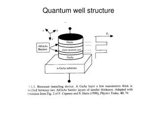
:Si SapphireSubstrate Sample • The excitation was by a continuous wave He-Cd laser • operating at 326nm and focused to 150 W/cm2. • The In0.04Ga0.96N:Si is a reference layer • The SQW well is 12nm below the Ag, well within the • penetration depth of the SP (40nm). • The Ag was deposited only on one half of the structure • so as to enable direct comparison of the PL spectrum. • The sample was at room temperature during the experiment. The PL was collected by a lens, dispersed by a monochromator and detected by a silicon photodiode.
Results • SQW PL peak at around 2.8eV • Second peak at around 3.17eV due, • attributed to the reference layer. • The curve B was obtained using Fresnel's • equation. • The curve C which is actual PL spectrum. • At 3.17eV, the curves C and B overlap. • At 2.8eV curve C is almost 2 orders less • than B, due to Plasmon Coupling. • Above 3.4eV there is a very strong • attenuation of the curve C, which is due • to the bulk Plasmon excitation. Absorption/reflection correction, Tp x TPL(ω) ≈ 0.5 Tp and TPL(ω) are obtained using Fresnel's equation.
Ratio of anticipated curve versus, actual • curve is shown. • Surface-Plasmon resonance centered at • 2.9eV with FWHM of 193meV. Q ≈ 15 • Due to bulk Plasmon resonance at 3.76 • there is a significant PL dip between • 3.4-3.6eV • Attenuation in external PL is not • due to absorption or reflection. • Its due to competition between • spontaneous emission into external • electromagnetic modes and Plasmon • modes.
Purcell Factor: A figure of merit for the cavity, which describes its ability to increase the coupling of an ideal emitter with the vacuum field. Fp is a analogues to Purcell factor, as it describes the ability of the metal film to Enhance coupling of the emitter (SQW) with the Plasmon modes. Г0 radiative recombination rate Гp recombination rate of spontaneous emission into Plasmon modes Гnr nonradiative recombination rate The nonradiative recombination rate is neglected, as the authors claim the quantum well is calibrated to have a quantum efficiency greater than 90%. • ρ(ħω), is the mode density of plasmons • d, local electron hole dipole moment • E(a), the local electric field of the plasmon • mode Fermi Golden Rule
L2 is the in-plane quantization area represents the energy density in a highly dispersive media. E(a) is normalized Can be obtained from the Dispersion curve of surface Plasmon. The factor 1/3 comes due to polarization averaging. Spontaneous emission rate for bulk semiconductor.
Good agreement between experimental and • theoretical Purcell factor. • Fp (Exp) = 56 ; Q (Exp) = 15 • Fp (The) = 49 ; Q (The) = 60 • Differences were attributed to the adjustable • parameter, Γnr that was dropped in theoretical • calculations.
Conclusions • Demonstrated direct coupling of electron and holes in SQW to • the thin Ag film. • The Purcell factor into the Plasmon mode competes well with • external spontaneous emission explaining the dip in PL spectra. • The Purcell factor could be further enhanced by the reducing the spacing between the • quantum well and the Ag film. • If the Ag film is incorporated with some antenna structure, it would be possible to • out-couple the SP. The result maybe a spontaneous emission which could be readily • extracted, and this spontaneous emission could compete more effectively with nonradiative • processes.
Related works • Showed that there is direct link between • the Plasmon resonance and enhanced PL • When the surface is structured, there is more • out-coupling of SP. Surface-plasmon-enhanced light emitters based on InGaN quantum wells, K Okamoto, I Niki, A Shvartser, Y Narukawa - Nature Materials, 2004