Download
1 / 18
200 likes | 448 Views
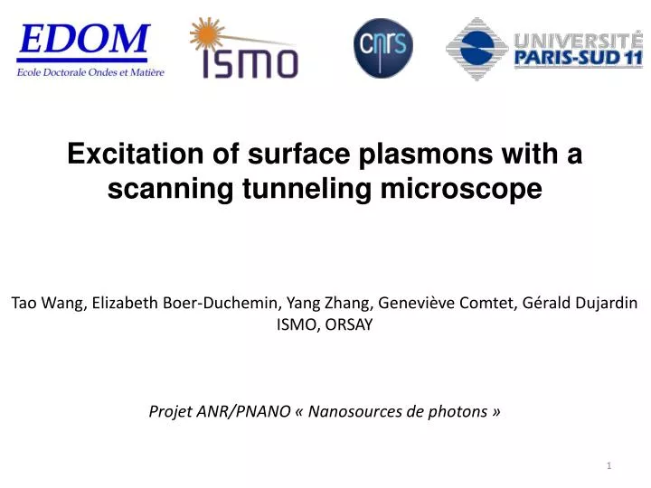
Excitation of surface plasmons with a scanning tunneling microscope Tao Wang, Elizabeth Boer-Duchemin, Yang Zhang, Geneviève Comtet, Gérald Dujardin ISMO, ORSAY Projet ANR/PNANO « Nanosources de photons ». 1. ω =ck 0. k SPP. Surface Plasmon Polariton. Surface plasmon polariton (SPP):

E N D
Excitation of surface plasmons with a scanning tunneling microscope Tao Wang, Elizabeth Boer-Duchemin, Yang Zhang, Geneviève Comtet, Gérald Dujardin ISMO, ORSAY Projet ANR/PNANO « Nanosources de photons » 1
ω=ck0 kSPP Surface Plasmon Polariton Surface plasmon polariton (SPP): EM wave confined at Metal-dielectric interface, coupled with oscillation of surface charges D ω0 z x M kspp > k0 λSPP <λ0, Beat the diffraction limit ! 2
Motivation Our experiment: surface plasmon excitation with a scanning tunneling microscope Surface plasmon excitation: usually with light laser k0 STM tip Kspp Kspp Kspp Kspp e- Our experiment isto dolocal electrical excitation of surface plasmons on a gold film by STM as a nanosource of photons. 3
Experiment setup STM head Inverted optical microscope 4
Experiments Experiment 1: thin gold film (35nm) Experiment 2: thin gold film (35nm) with gold nanoparticles(NPs) Experiment 3: thick gold film (200nm) with holes
Experiment 1: STM excited on thin gold film (35nm) Image plane image with oil objective oil objective100X, NA=1.45 W tip, 2.5V, 6nA 10 μm Image plane Surface plasmon propagates on the gold film 6 Gold films deposition in IEF CTU, Orsay
Experiment 1: STM excited on thin gold film (35nm) Fourier plane f f Fourier plane R R=n×sin (θ)×f 7
Experiment 1: STM excited on thin gold film (35nm) Fourier plane images with oil objective oil objective100X, NA=1.45 W tip, 2.5V, 6nA kspp nk0 θspp R Surface plasmons emit at large angles (related to leakage radiation coupling) Fourier plane Coupling condition : kspp=nk0 sin(θspp) kspp›k0, sin(θspp)=kspp/nk0›1/n, θspp›critical angle 8
Experiment 1: STM excited on thin gold film (35nm) Spectra measurement
Experiment 1: STM excited on thin gold film (35nm) Conclusion STM can excite propagating surface plasmon on the gold film (broad spectra band) Propagating surface plasmons emit at large angles This will be published on nanotechnology soon.
Experiment 2: thin Au film (35nm) with Au NPs STM topography image (9μm×9μm) 500nm NP1 Tip position NP2 NP1 NP2 Collaboration with Prof. Hynd Remita (LCP, Orsay)
Experiment 2: thin Au film (35nm) with Au NPs Preliminary results image plane image 9μm×9μm
Experiment 2: thin Au film (35nm) with Au NPs Preliminary conclusion STM excite propagating surface plasmon on the gold film Propagating surface plasmon scattered by the Au NPs
Experiment 3: thick gold film (200nm) with nanoholes STM Topography image (6μm×6μm) 3μm Collaboration with Serge Huant (Néel, Grenoble)
Experiment 3: thick gold film (200nm) with nanoholes Preliminary results STM excited light emission image 5μm
Experiment 3: thick gold film (200nm) with nanoholes Preliminary conclusion STM excite propagating surface plasmon on the gold film Propagating surface plasmon scattered by the nanoholes
Conclusions and future work Experiment 1: thin gold film (35nm) Experiment 2: thin gold film (35nm) with gold nanoparticles(NPs) Experiment 3: thick gold film (200nm) with holes