Download
1 / 20
200 likes | 398 Views
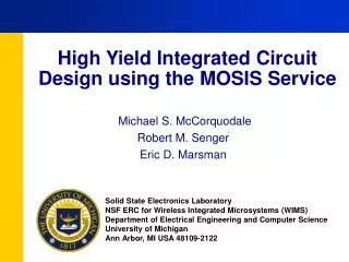
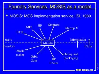
Stanford. HP. MIT. Startup X. UCB. users. Information. vendors. Chips. Mask maker. Dicing and packaging. Orbit 2um. HP 0.5um. Foundry Services: MOSIS as a model. MOSIS: MOS implementation service, ISI, 1980. MOSIS. $$$$$. Foundry Services and Standard Processes.

E N D
Stanford HP MIT Startup X UCB users Information vendors Chips Mask maker Dicing and packaging Orbit 2um HP 0.5um Foundry Services: MOSIS as a model • MOSIS: MOS implementation service, ISI, 1980. MOSIS $$$$$
Foundry Services and Standard Processes • MCNC/MUMPS (now by Cronos) • 3 level poly, no electronics • started in 1992, now 6 runs per year • LIGAMUMPS • single level metal, no electronics • Sandia • 5 level poly, no electronics • 1 level poly w/ quality CMOS • CMOS + post-processing • EDP, TMAH, XeF2 (Parameswaran) • Plasma (Fedder)
Design “Rules” • Guidelines for communication between fab people and design people • Generally not enforced • MUMPS, 2um CMOS: no • HP sub-micron CMOS: yes • Often desireable to violate • MUMPS: process exploration, new devices, some previous design rule violations are now encouraged • CMOS: Parameswaran, Fedder style MEMS depends on design rule violations
Line width ... and spacing Design Rules • Typically due to • lithographic resolution limits • lithographic alignment repeatability • etching capabilities • Most important: Line/space • due to lithography or etching • varies from layer to layer • varies near topography • no guarantee of dimensions: the lines will exist and be distinct.
MCNC/MUMPS Design Rules Rules for line/space on all mask layers.
MCNC/MUMPS Design Rules Examples for POLY2 from mems.mcnc.org/smumps/mrules
Breaking the Rules • Sub-minimum lithography • risky, but often successful, especially in planar areas • Breaching nitride (substrate contacts and opens) • Stack anchor1 and poly1-poly2-via • don’t include poly1 • include poly2 for electrical contact to substrate, or remove to expose bare substrate • Double-thick poly • continuous sheet of poly1 enclosed in poly1-poly2-via • poly2 structures on top
MCNC/MUMPS access • Cost is $3,500 per submission • 1cm2 die area per submission • 15 identical dice returned (~$2/mm2) • Files are submitted by anonymous ftp • Dicing, bonding, HF release are all available for additional cost • Parameterized and static design cells are free online (CaMEL) • Design services are available for additional cost
MCNC/MUMPS process specs Polys are compressive, nitride and metal (Cr/Au) are tensile.
MCNC/LIGAMUMPS Design Rules A, W, L must be greater than or equal to 20.0 microns. Photoresist aspect ratio, L/W, must be less than or equal to 10.