Download
1 / 36
360 likes | 516 Views
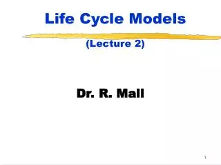
361 Computer Architecture Lecture 9: Designing Single Cycle Control. 31. 26. 21. 16. 11. 6. 0. op. rs. rt. rd. shamt. funct. 6 bits. 5 bits. 5 bits. 5 bits. 5 bits. 6 bits. 31. 26. 21. 16. 0. op. rs. rt. immediate. 6 bits. 5 bits. 5 bits. 16 bits. 31. 26. 0. op.

E N D
361Computer ArchitectureLecture 9: Designing Single Cycle Control
31 26 21 16 11 6 0 op rs rt rd shamt funct 6 bits 5 bits 5 bits 5 bits 5 bits 6 bits 31 26 21 16 0 op rs rt immediate 6 bits 5 bits 5 bits 16 bits 31 26 0 op target address 6 bits 26 bits Recap: The MIPS Subset • ADD and subtract • add rd, rs, rt • sub rd, rs, rt • OR Imm: • ori rt, rs, imm16 • LOAD and STORE • lw rt, rs, imm16 • sw rt, rs, imm16 • BRANCH: • beq rs, rt, imm16 • JUMP: • j target
Recap: A Single Cycle Datapath • We have everything except control signals (underline) • Today’s lecture will show you how to generate the control signals Instruction<31:0> Branch Instruction Fetch Unit Jump Rd Rt <21:25> <16:20> <11:15> <0:15> Clk RegDst 1 0 Mux Rt Rs Rd Imm16 Rs Rt RegWr ALUctr 5 5 5 MemtoReg busA Zero MemWr Rw Ra Rb busW 32 32 32-bit Registers 0 ALU 32 busB 32 0 Clk Mux 32 Mux 32 1 WrEn Adr 1 Data In 32 Data Memory Extender imm16 32 16 Clk ALUSrc ExtOp
Processor Input Control Memory Datapath Output The Big Picture: Where are We Now? • The Five Classic Components of a Computer • Today’s Topic: Designing the Control for the Single Cycle Datapath
Outline of Today’s Lecture • Recap and Introduction • Control for Register-Register & Or Immediate instructions • Control signals for Load, Store, Branch, & Jump • Building a local controller: ALU Control • The main controller • Summary
31 26 21 16 11 6 0 op rs rt rd shamt funct 6 bits 5 bits 5 bits 5 bits 5 bits 6 bits RTL: The ADD Instruction • add rd, rs, rt • mem[PC] Fetch the instruction from memory • R[rd] <- R[rs] + R[rt] The actual operation • PC <- PC + 4 Calculate the next instruction’s address
1 Mux PC 0 0 Adder Mux 1 Adder Clk Instruction Fetch Unit at the Beginning of Add / Subtract • Fetch the instruction from Instruction memory: Instruction <- mem[PC] • This is the same for all instructions 30 Addr<31:2> 30 PC<31:28> Addr<1:0> “00” 4 Target Instruction Memory 30 Instruction<25:0> 26 30 32 30 “1” Jump = previous Instruction<31:0> 30 SignExt 30 imm16 16 Instruction<15:0> Branch = previous Zero = previous
31 26 21 16 11 6 0 op rs rt rd shamt funct The Single Cycle Datapath during Add and Subtract • R[rd] <- R[rs] + / - R[rt] Instruction<31:0> Branch = 0 Instruction Fetch Unit Jump = 0 Rd Rt <21:25> <16:20> <11:15> <0:15> Clk RegDst = 1 1 0 Mux ALUctr = Add or Subtract Rt Rs Rd Imm16 Rs Rt RegWr = 1 5 5 5 MemtoReg = 0 busA Zero MemWr = 0 Rw Ra Rb busW 32 32 32-bit Registers 0 ALU 32 busB 32 0 Clk Mux 32 Mux 32 1 WrEn Adr 1 Data In 32 Data Memory Extender imm16 32 16 Clk ALUSrc = 0 ExtOp = x
1 Mux PC 0 0 Adder Mux 1 Adder Clk Instruction Fetch Unit at the End of Add and Subtract • PC <- PC + 4 • This is the same for all instructions except: Branch and Jump 30 Addr<31:2> 30 PC<31:28> Addr<1:0> “00” 4 Target Instruction Memory 30 Instruction<25:0> 26 30 32 30 “1” Jump = 0 Instruction<31:0> 30 SignExt 30 imm16 16 Instruction<15:0> Branch = 0 Zero = x
31 26 21 16 0 op rs rt immediate The Single Cycle Datapath during Or Immediate • R[rt] <- R[rs] or ZeroExt[Imm16] Instruction<31:0> nPC_sel= +4 Instruction Fetch Unit Rd Rt <21:25> <16:20> <11:15> <0:15> Clk RegDst = 0 1 0 Mux Rt Rs Rd Imm16 Rs Rt ALUctr = Or RegWr = 1 MemtoReg = 0 5 5 5 busA Zero MemWr = 0 Rw Ra Rb busW 32 32 32-bit Registers 0 ALU 32 busB 32 0 Clk Mux 32 Mux 32 1 WrEn Adr 1 Data In 32 Data Memory Extender imm16 32 16 Clk ALUSrc = 1 ExtOp = 0
31 26 21 16 0 op rs rt immediate The Single Cycle Datapath during Load • R[rt] <- Data Memory {R[rs] + SignExt[imm16]} Instruction<31:0> nPC_sel= +4 Instruction Fetch Unit Rd Rt <21:25> <16:20> <11:15> <0:15> Clk RegDst = 0 1 0 Mux ALUctr = Add Rt Rs Rd Imm16 Rs Rt RegWr = 1 MemtoReg = 1 5 5 5 busA Zero MemWr = 0 Rw Ra Rb busW 32 32 32-bit Registers 0 ALU 32 busB 32 0 Clk Mux 32 Mux 1 WrEn Adr 1 Data In 32 Data Memory Extender 32 imm16 32 16 Clk ALUSrc = 1 ExtOp = 1
31 26 21 16 0 op rs rt immediate The Single Cycle Datapath during Store • Data Memory {R[rs] + SignExt[imm16]} <- R[rt] Instruction<31:0> nPC_sel= +4 Instruction Fetch Unit Rd Rt <21:25> <16:20> <11:15> <0:15> Clk RegDst = x 1 0 Mux ALUctr = Add Rt Rs Rd Imm16 Rs Rt RegWr = 0 5 5 5 MemtoReg = x busA Zero MemWr = 1 Rw Ra Rb busW 32 32 32-bit Registers 0 ALU 32 busB 32 0 Clk Mux 32 Mux 32 1 WrEn Adr 1 32 Data In Data Memory Extender imm16 32 16 Clk ALUSrc = 1 ExtOp = 1
31 26 21 16 0 op rs rt immediate The Single Cycle Datapath during Branch • if (R[rs] - R[rt] == 0) then Zero <- 1 ; else Zero <- 0 Instruction<31:0> Branch = 1 Instruction Fetch Unit Jump = 0 Rd Rt <21:25> <16:20> <11:15> <0:15> Clk RegDst = x 1 0 Mux ALUctr = Subtract Rt Rs Rd Imm16 Rs Rt RegWr = 0 MemtoReg = x 5 5 5 busA Zero MemWr = 0 Rw Ra Rb busW 32 32 32-bit Registers 0 ALU 32 busB 32 0 Clk Mux 32 Mux 32 1 WrEn Adr 1 Data In 32 Data Memory Extender imm16 32 16 Clk ALUSrc = 0 ExtOp = x
31 26 21 16 0 op rs rt immediate 1 Mux PC 0 0 Adder Mux 1 Adder Clk Instruction Fetch Unit at the End of Branch • if (Zero == 1) then PC = PC + 4 + SignExt[imm16]*4 ; else PC = PC + 4 30 Addr<31:2> 30 PC<31:28> Addr<1:0> “00” 4 Target Instruction Memory 30 Instruction<25:0> 26 30 32 30 “1” Jump = 0 Instruction<31:0> 30 SignExt 30 imm16 16 Assume Zero = 1 to see the interesting case. Instruction<15:0> Branch = 1 Zero = 1
31 26 0 op target address The Single Cycle Datapath during Jump • Nothing to do! Make sure control signals are set correctly! Instruction<31:0> Branch = 0 Instruction Fetch Unit Jump = 1 Rd Rt <21:25> <16:20> <11:15> <0:15> Clk RegDst = x 1 0 Mux Rt Rs Rd Imm16 ALUctr = x Rs Rt RegWr = 0 5 5 5 MemtoReg = x busA Zero MemWr = 0 Rw Ra Rb busW 32 32 32-bit Registers 0 ALU 32 busB 32 0 Clk Mux 32 Mux 32 1 WrEn Adr 1 Data In 32 Data Memory Extender imm16 32 16 Clk ALUSrc = x ExtOp = x
31 26 0 op target address 1 Mux PC 0 0 Adder Mux 1 Adder Clk Instruction Fetch Unit at the End of Jump • PC <- PC<31:29> concat target<25:0> concat “00” 30 Addr<31:2> 30 PC<31:28> Addr<1:0> “00” 4 Target Instruction Memory 30 Instruction<25:0> 26 30 32 30 “1” Jump = 1 Instruction<31:0> 30 SignExt 30 imm16 16 Instruction<15:0> Branch = 0 Zero = x
Step 4: Given Datapath: RTL -> Control Instruction<31:0> Inst Memory <21:25> <21:25> <16:20> <11:15> <0:15> Adr Op Fun Rt Rs Rd Imm16 Control ALUctr nPC_sel MemWr MemtoReg ALUSrc RegWr RegDst ExtOp Equal DATA PATH
A Summary of Control Signals inst Register Transfer ADD R[rd] <– R[rs] + R[rt]; PC <– PC + 4 ALUsrc = RegB, ALUctr = “add”, RegDst = rd, RegWr, nPC_sel = “+4” SUB R[rd] <– R[rs] – R[rt]; PC <– PC + 4 ALUsrc = RegB, ALUctr = “sub”, RegDst = rd, RegWr, nPC_sel = “+4” ORi R[rt] <– R[rs] + zero_ext(Imm16); PC <– PC + 4 ALUsrc = Im, Extop = “Z”, ALUctr = “or”, RegDst = rt, RegWr, nPC_sel = “+4” LOAD R[rt] <– MEM[ R[rs] + sign_ext(Imm16)]; PC <– PC + 4 ALUsrc = Im, Extop = “Sn”, ALUctr = “add”, MemtoReg, RegDst = rt, RegWr, nPC_sel = “+4” STORE MEM[ R[rs] + sign_ext(Imm16)] <– R[rs]; PC <– PC + 4 ALUsrc = Im, Extop = “Sn”, ALUctr = “add”, MemWr, nPC_sel = “+4” BEQ if ( R[rs] == R[rt] ) then PC <– PC + sign_ext(Imm16)] || 00 else PC <– PC + 4 nPC_sel = “Br”, ALUctr = “sub”
add sub ori lw sw beq jump RegDst 1 0 0 0 x x x ALUSrc 0 0 1 1 1 0 x MemtoReg 0 0 0 1 x x x RegWrite 1 1 1 1 0 0 0 MemWrite 0 0 0 0 1 0 0 Branch 0 0 0 0 0 1 0 Jump 0 0 0 0 0 0 1 ExtOp x x 0 1 1 x x ALUctr<2:0> Add Subtract Or Add Add xxx Subtract 31 26 21 16 11 6 0 op rs rt rd shamt funct immediate op rs rt op target address A Summary of the Control Signals See func 10 0000 10 0010 We Don’t Care :-) Appendix A op 00 0000 00 0000 00 1101 10 0011 10 1011 00 0100 00 0010 R-type add, sub I-type ori, lw, sw, beq J-type jump
op 00 0000 00 1101 10 0011 10 1011 00 0100 00 0010 R-type ori lw sw beq jump RegDst 1 0 0 x x x ALUSrc 0 1 1 1 0 x MemtoReg 0 0 1 x x x RegWrite 1 1 1 0 0 0 MemWrite 0 0 0 1 0 0 Branch 0 0 0 0 1 0 Jump 0 0 0 0 0 1 ExtOp x 0 1 1 x x ALUop<N:0> “R-type” Or Add Add xxx Subtract ALU Control (Local) The Concept of Local Decoding func ALUctr op 6 Main Control 3 ALUop 6 N ALU
func ALU Control (Local) op 6 ALUctr Main Control ALUop 6 3 N The Encoding of ALUop • In this exercise, ALUop has to be 2 bits wide to represent: • (1) “R-type” instructions • “I-type” instructions that require the ALU to perform: • (2) Or, (3) Add, and (4) Subtract • To implement the full MIPS ISA, ALUop hat to be 3 bits to represent: • (1) “R-type” instructions • “I-type” instructions that require the ALU to perform: • (2) Or, (3) Add, (4) Subtract, and (5) And (Example: andi) R-type ori lw sw beq jump ALUop (Symbolic) “R-type” Or Add Add xxx Subtract ALUop<2:0> 1 00 0 10 0 00 0 00 xxx 0 01
func ALU Control (Local) op 6 ALUctr Main Control ALUop 6 3 N R-type ori lw sw beq jump ALUop (Symbolic) “R-type” Or Add Add xxx Subtract ALUop<2:0> 1 00 0 10 0 00 0 00 xxx 0 01 31 26 21 16 11 6 0 R-type op rs rt rd shamt funct funct<5:0> Instruction Operation ALUctr ALUctr<2:0> ALU Operation 10 0000 add 000 Add 10 0010 subtract 001 Subtract 10 0100 and 010 And ALU 10 0101 or 110 Or 10 1010 set-on-less-than 111 Set-on-less-than The Decoding of the “func” Field ( P. 286 text)
R-type ori lw sw beq ALUop (Symbolic) “R-type” Or Add Add Subtract ALUop<2:0> 1 00 0 10 0 00 0 00 0 01 ALUop func ALU Operation ALUctr bit<2> bit<1> bit<0> bit<3> bit<2> bit<1> bit<0> bit<2> bit<1> bit<0> 0 0 0 x x x x Add 0 1 0 0 x 1 x x x x Subtract 1 1 0 0 1 x x x x x Or 0 0 1 1 x x 0 0 0 0 Add 0 1 0 1 x x 0 0 1 0 Subtract 1 1 0 1 x x 0 1 0 0 And 0 0 0 1 x x 0 1 0 1 Or 0 0 1 1 x x 1 0 1 0 Set on < 1 1 1 The Truth Table for ALUctr funct<3:0> Instruction Op. 0000 add 0010 subtract 0100 and 0101 or 1010 set-on-less-than
The Logic Equation for ALUctr<2> ALUop func bit<2> bit<1> bit<0> bit<3> bit<2> bit<1> bit<0> ALUctr<2> • ALUctr<2> = !ALUop<2> & ALUop<0> + ALUop<2> & !func<2> & func<1> & !func<0> 0 x 1 x x x x 1 1 x x 0 0 1 0 1 1 x x 1 0 1 0 1 X Y Z A B C D This makes func<3> a don’t care = !X&Y + X&!A&!B&C&!D + X&A&!B&C&!D = !X&Y + X&!B&C&!D
The Logic Equation for ALUctr<1> ALUop func bit<2> bit<1> bit<0> bit<3> bit<2> bit<1> bit<0> ALUctr<1> • ALUctr<1> = !ALUop<2> & !ALUop<0> + ALUop<2> & !func<2> & !func<0> 0 0 0 x x x x 1 0 x 1 x x x x 1 1 x x 0 0 0 0 1 1 x x 0 0 1 0 1 1 x x 1 0 1 0 1
The Logic Equation for ALUctr<0> ALUop func bit<2> bit<1> bit<0> bit<3> bit<2> bit<1> bit<0> ALUctr<0> • ALUctr<0> = !ALUop<2> & ALUop<0> + ALUop<2> & !func<3> & func<2> & !func<1> & func<0> + ALUop<2> & func<3> & !func<2> & func<1> & !func<0> 0 1 x x x x x 1 1 x x 0 1 0 1 1 1 x x 1 0 1 0 1
func ALU Control (Local) 6 ALUctr ALUop 3 3 The ALU Control Block • ALUctr<2> = !ALUop<2> & ALUop<0> + ALUop<2> & !func<2> & func<1> & !func<0> • ALUctr<1> = !ALUop<2> & !ALUop<0> + ALUop<2> & !func<2> & !func<0> • ALUctr<0> = !ALUop<2> & ALUop<0> + ALUop<2> & !func<3> & func<2> & !func<1> & func<0> + ALUop<2> & func<3> & !func<2> & func<1> & !func<0>
Step 5: Logic for each control signal • nPC_sel <= if (OP == BEQ) then EQUAL else 0 • ALUsrc <= if (OP == “Rtype”) then “regB” else “immed” • ALUctr <= if (OP == “Rtype”) then funct elseif (OP == ORi) then “OR” elseif (OP == BEQ) then “sub” else “add” • ExtOp <= _____________ • MemWr <= _____________ • MemtoReg <= _____________ • RegWr: <=_____________ • RegDst: <= _____________
RegDst func ALUSrc ALUctr ALU Control (Local) op 6 Main Control : 3 6 ALUop 3 The “Truth Table” for the Main Control op 00 0000 00 1101 10 0011 10 1011 00 0100 00 0010 R-type ori lw sw beq jump RegDst 1 0 0 x x x ALUSrc 0 1 1 1 0 x MemtoReg 0 0 1 x x x RegWrite 1 1 1 0 0 0 MemWrite 0 0 0 1 0 0 Branch 0 0 0 0 1 0 Jump 0 0 0 0 0 1 ExtOp x 0 1 1 x x ALUop (Symbolic) “R-type” Or Add Add xxx Subtract ALUop <2> 1 0 0 0 x 0 ALUop <1> 0 1 0 0 x 0 ALUop <0> 0 0 0 0 x 1
. . . . . . op<5> op<5> op<5> op<5> op<5> op<5> . . . . . . <0> <0> <0> <0> <0> op<0> R-type ori lw sw beq jump The “Truth Table” for RegWrite op 00 0000 00 1101 10 0011 10 1011 00 0100 00 0010 R-type ori lw sw beq jump • RegWrite = R-type + ori + lw = !op<5> & !op<4> & !op<3> & !op<2> & !op<1> & !op<0> (R-type) + !op<5> & !op<4> & op<3> & op<2> & !op<1> & op<0> (ori) + op<5> & !op<4> & !op<3> & !op<2> & op<1> & op<0> (lw) RegWrite 1 1 1 x x x RegWrite
. . . . . . op<5> op<5> op<5> op<5> op<5> op<5> . . . . . . <0> <0> <0> <0> <0> op<0> R-type ori lw sw beq jump PLA Implementation of the Main Control RegWrite ALUSrc RegDst MemtoReg MemWrite Branch Jump ExtOp ALUop<2> ALUop<1> ALUop<0>
Putting it All Together: A Single Cycle Processor ALUop ALU Control ALUctr 3 RegDst func op 3 Main Control Instr<5:0> 6 ALUSrc 6 : Instr<31:26> Instruction<31:0> Branch Instruction Fetch Unit Jump Rd Rt <21:25> <16:20> <11:15> <0:15> Clk RegDst 1 0 Mux Rt Rs Rd Imm16 Rs Rt RegWr ALUctr 5 5 5 MemtoReg busA Zero MemWr Rw Ra Rb busW 32 32 32-bit Registers 0 ALU 32 busB 32 0 Clk Mux 32 Mux 32 1 WrEn Adr 1 Data In 32 Data Memory Extender imm16 32 16 Instr<15:0> Clk ALUSrc ExtOp
. . . . . . . . . . . . Clocking Methodology Clk Setup Hold Setup Hold • All storage elements are clocked by the same clock edge • Cycle Time = CLK-to-Q + Longest Delay Path + Setup + Clock Skew • (CLK-to-Q + Shortest Delay Path - Clock Skew) > Hold Time Don’t Care
Worst Case Timing (Load) Clk Clk-to-Q Old Value New Value PC Instruction Memoey Access Time Rs, Rt, Rd, Op, Func Old Value New Value Delay through Control Logic ALUctr Old Value New Value ExtOp Old Value New Value ALUSrc Old Value New Value MemtoReg Old Value New Value Register Write Occurs RegWr Old Value New Value Register File Access Time busA Old Value New Value Delay through Extender & Mux busB Old Value New Value ALU Delay Address Old Value New Value Data Memory Access Time busW Old Value New
Drawback of this Single Cycle Processor • Long cycle time: • Cycle time must be long enough for the load instruction: PC’s Clock -to-Q + Instruction Memory Access Time + Register File Access Time + ALU Delay (address calculation) + Data Memory Access Time + Register File Setup Time + Clock Skew • Cycle time is much longer than needed for all other instructions
Processor Input Control Memory Datapath Output Summary • Single cycle datapath => CPI=1, CCT => long • 5 steps to design a processor • 1. Analyze instruction set => datapath requirements • 2. Select set of datapath components & establish clock methodology • 3. Assemble datapath meeting the requirements • 4. Analyze implementation of each instruction to determine setting of control points that effects the register transfer. • 5. Assemble the control logic • Control is the hard part • MIPS makes control easier • Instructions same size • Source registers always in same place • Immediates same size, location • Operations always on registers/immediates

![Computer Architecture & Operating System [O.S.]](https://cdn0.slideserve.com/35278/computer-architecture-operating-system-o-s-dt.jpg)