Download
1 / 46
460 likes | 703 Views
Chapter 3B EGR 270 – Fundamentals of Computer Engineering. 1. Reading Assignment: Chapter 3B in Logic and Computer Design Fundamentals, 4 th Edition by Mano . Combinational Functions and Circuits

E N D
Chapter 3B EGR 270 – Fundamentals of Computer Engineering 1 Reading Assignment:Chapter 3B in Logic and Computer Design Fundamentals, 4th Edition by Mano • Combinational Functions and Circuits • Functions and fundamental circuits are introduced in this chapter which are useful in designing larger digital circuits. • These circuits are presented as functional blocks – fundamental, reusable circuits. The focus is to develop the functional blocks such that they are reusable, are easily expanded for use with larger functions, and are efficiently designed for implementing via VHDL programming. • Examples of functional blocks to be introduced: • Decoders • Encoders • Priority encoders • Multiplexers • De-multiplexers • Magnitude Comparators • Programmable Logic (Chapter 6)
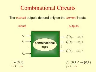
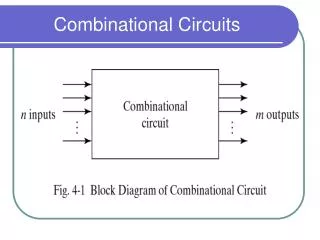
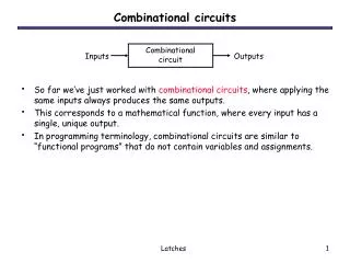
Chapter 3B EGR 270 – Fundamentals of Computer Engineering 2 Combinational Logic Using MSI and LSI devices Although our focus will be more on defining functional blocks that are designed to be reusable and to be implemented using VHDL, many of these fundamental circuits are also available as commercially available IC’s. Commercial devices can perform complex functions using perhaps a single IC, thus saving space. They are typically faster that equivalent circuits that we might build using discrete logic gates. It might be a good idea to browse through a Logic Data Book to see what is available. A few devices are listed below. Assortment of commercially available combinational logic devices
Chapter 3B EGR 270 – Fundamentals of Computer Engineering 3 Decoders An N-bit decoder has 2N outputs, only one of which may be activated at a given time. If the device is active-HIGH , then only one output may be HIGH at any time. If the device is active-LOW , then only one output may be LOW at any time. Example: A 3-bit decoder might also be called a 3-line-to-8-line decoder or a 3x8 decoder. The block diagram is shown below: • Discuss: • basic operation • the truth table
Chapter 3B EGR 270 – Fundamentals of Computer Engineering 4 Active-LOW versus Active-HIGH decoders Enable lines – essentially act as ON/OFF switches Example: Show the truth table and block diagram for an active-LOW 2x4 decoder with an enable line, E.
Chapter 3B EGR 270 – Fundamentals of Computer Engineering 5 Circuit Design Show that decoder outputs are essentially minterms and draw a circuit for a 2x4 decoder (no enable, active-HIGH outputs)
Chapter 3B EGR 270 – Fundamentals of Computer Engineering 6 Decoder expansion using hierarchy The text introduces a procedure for forming any (n x 2n) decoder by expanding smaller decoders. The result requires only 2-input AND gates (rather than n-input) and inverters. This technique is especially useful for building large decoders using reusable fundamental blocks. Figure 3-19 below illustrates a 3x8 decoder constructed using this method:
Chapter 3B EGR 270 – Fundamentals of Computer Engineering 7 Implementing Boolean functions using decoders Note that the decoder outputs for active-HIGH decoders are simply minterms, so F = (minterms) = (active-HIGH decoder outputs) Example: Implement f(A,B,C) = (0, 3, 5, 6) using a 3 x 8 decoder with active-HIGH outputs Note that the decoder outputs for active-LOW decoders are simply maxterms, so F = (maxterms) = (active-LOW decoder outputs) Example: Implement f(A,B,C) = (0, 3, 5, 6) using a 3 x 8 decoder with active-LOW outputs
Chapter 3B EGR 270 – Fundamentals of Computer Engineering 8 • Decoder IC’s • 74155 Data Sheet (dual 2x4 decoder/single 3x8 decoder) – see next slide • How many enable lines does the 74155 have? Are they active-LOW or active-HIGH? (study the truth table on the next slide) • Is B is MSB or LSB? (check the data sheet on the next slide) 1C 1G 1Y0 1Y1 1Y2 1Y3 B A Note: The 74156 is similar to the 74155 except that it has open-collector outputs instead of totem-pole outputs. Discuss the advantage of this (recall from Lab 2 that if open-collector outputs are tied together, they are ANDed). B A 74155 2Y0 2Y1 2Y2 2Y3 B A 2C 2G
Chapter 3B EGR 270 – Fundamentals of Computer Engineering 9
Chapter 3B EGR 270 – Fundamentals of Computer Engineering 10 • 74155 connected as a 2x4 decoder • Label the outputs below. Which 2x4 decoder is being used? 1 0 1C 1G 1Y0 1Y1 1Y2 1Y3 B A 1 0 B A 74155 2Y0 2Y1 2Y2 2Y3 B A 2C 2G 1 0
Chapter 3B EGR 270 – Fundamentals of Computer Engineering 11 • 74155 connected as a 3x8 decoder • Show how to connect inputs C, B, and A. • Label the outputs D0, D1, …, D7 (they are NOT in order!) • Add an example (pick some input and label all outputs) 1C 1G 1Y0 1Y1 1Y2 1Y3 B A B A 74155 2Y0 2Y1 2Y2 2Y3 B A 2C 2G
Chapter 3B EGR 270 • 74155 connected as a 4x16 decoder • Show how to connect inputs D, C, B, and A. Note that one NOT gate will be needed. • Label the outputs D0, D1, …, D15 (they are NOT in order!) • Add an example (pick some input and label all outputs) 1C 1G 1C 1G 1Y0 1Y1 1Y2 1Y3 1Y0 1Y1 1Y2 1Y3 B A B A B A B A 74155 74155 2Y0 2Y1 2Y2 2Y3 2Y0 2Y1 2Y2 2Y3 B A B A 2C 2G 2C 2G 12
Chapter 3B EGR 270 – Fundamentals of Computer Engineering 13 I0 I1 22 x I2 8 x 3 Encoder I3 Output Code 21 y I4 20 z I5 I6 I7 Encoder An encoder is essentially the opposite of a decoder. An N-bit encoder has 2N inputs lines, one of which is active, and N output lines that carry the binary code corresponding to the active input. The 8 x 3 encoder shown below might also be called an octal-to-binary encoder. Only one input may be activated (active-HIGH inputs shown) Example: Add a set of valid binary values to the input and show the corresponding output.
Chapter 3B EGR 270 – Fundamentals of Computer Engineering 14 Note that encoders and decoders perform the opposite functions. Example: Show an 4x2 encoder followed by a 2x4 decoder with some sample inputs and outputs. Example: Show a 2x4 decoder followed by an 4x2 encoder with some sample inputs and outputs.
Chapter 3B EGR 270 – Fundamentals of Computer Engineering 15 Encoder Truth Table Draw the truth tablefor an 8x3 encoder. From the truth table, determine expressions for the outputs x, y, and z. (List only the 8 valid inputs, not all 256 combinations.)
Chapter 3B EGR 270 – Fundamentals of Computer Engineering 16 I0 I1 22 x I2 8 x 3 Encoder I3 Output Code 21 y I4 20 z I5 I6 I7 Encoder – adding a Valid output line, V Valid Output? One problem with the encoder design above is that there is no way to indicate that an invalid input occurred. This problem can be resolved by using an additional output called a valid line, V. V V = 1 for a valid code (0 if invalid)
Chapter 3B EGR 270 – Fundamentals of Computer Engineering 17 • Basic Encoder Design • Note that if the input is valid, the x = 1 when I4, I5, I6, or I7 = 1. So: • V = 1 only for the 8 valid input combinations, so: • Draw the circuit
Chapter 3B EGR 270 – Fundamentals of Computer Engineering 18 Decoders and Encoders - Applications Decoders can be used to reduce the number of wires needed to control multiple outputs. Encoders can be used to reduce the number of wires needed to read multiple inputs. These wires might be to external devices or might be within a digital circuit. • Encoder Example 1 – Reading 256 external sensors with a computer • Suppose that a computer was used to read the status of 256 sensors in a special application where only one sensor would ever be HIGH at a given time. • One option would be to find a 256-pin connector to work with the computer (good luck). • A better option would be to use an 256x8 encoder and use an 8-bit connector on the computer. The computer could then simply read the code to determine which sensor was activated. • Encoder Example 2 – Reading a keyboard • Encoders are also used in keyboards. • Rather than send over 100 different signals from the keyboard corresponding to the key that has been pressed, the keys are encoded using an ASCII code. • A 7-bit ASCII code is sufficient to represent all keys along with a 128x7 encoder.
Chapter 3B EGR 270 – Fundamentals of Computer Engineering 19 32 x 5 Encoder . . . Encoder Example 3: IEEE sponsors competitions for students in electrical and computer engineering. In a prior IEEE SouthEastConsoftware competition held at Virginia Tech, Computer Engineering students were given the challenge of designing a program to control an HO-scale train. A track was set up with 32 sensors. A sensor would read HIGH when the train was over it and LOW otherwise. A 32x5 encoder was used to encode the sensor information. The train, track, sensors, and encoder were provided and the distance between the sensors was specified. Student teams had to write software to: 1) stop and start the train at any sensor location 2) execute a planned train route 3) display the speed of the train etc.
Chapter 3B EGR 270 – Fundamentals of Computer Engineering 20 • Decoder Example: • A few years ago TCC worked with ODU, William & Mary, and Hampton University on the Virginia Student Balloon Launch (VSBL) Program. • NASA sponsors a number of such projects, where NASA engineers provide a high-altitude balloon (up to 100,000 ft) and engineering students at colleges and universities design experiments for the upper atmosphere. • In one experiment William and Mary students provided 8 stainless steel cylinders that were pumped to a vacuum just before liftoff. The valve on each cylinder was opened briefly at precise altitudes so that they would suck in a sample of the air which was analyzed after landing to detect the presence of certain pollutants. • The onboard computer could have tied up 8 output lines to control the 8 cylinders, but instead used a 3x8 decoder and thus only used 3 output lines.
Chapter 3B EGR 270 – Fundamentals of Computer Engineering 21 Highest priority I7 I6 . . . . 22 x I5 8x3 Priority Encoder I4 Output 21 y I3 Code 20 z I2 I1 V = 1 for a valid code (0 if invalid) V Lowest priority I0 • Priority Encoder • A priority encoder is an encoder where: • more than one input may be activated • each input is assigned a priority • the output code corresponds to the highest priority input that has been activated. Example: Add a set of valid binary values to the input (with 2 or more active) and show the corresponding output.
Chapter 3B EGR 270 – Fundamentals of Computer Engineering 22 Example: Show the truth table for an 8x3 priority encoder with an output line V with active-HIGH inputs and outputs. (Only 9 lines are needed in the truth table if you make use of don’t cares.) How many invalid inputs are possible?
Chapter 3B EGR 270 – Fundamentals of Computer Engineering 23 Magnitude Comparators A magnitude comparator is used to compare two binary inputs. The output will indicate if the inputs are equal or which input is larger. Comparing for equality (also discussed earlier) 1-bit comparison for equality: 4-bit comparison for equality: Two 4-bit words A = A3A2A1A0 and B = B3B2B1B0 are equal if A3 = B3 , A2 = B2 , etc.
Chapter 3B EGR 270 – Fundamentals of Computer Engineering 24 Comparing to determine if A > B, A < B, or A = B A typical block diagram for a 4-bit comparator is shown to the right. • Algorithm for A > B: • A > B if A3 = 1 and B3 = 0, (A3' B3) • A > B if A3 = B3 (i.e., x3 - see previous page) and A2 = 1 and B2 = 0, (x3A2' B2) • So: • Similarly:
Chapter 3B EGR 270 – Fundamentals of Computer Engineering 25 Diagram for 4-bit comparator based on algorithm’s developed on the last two slides:
Chapter 3B EGR 270 – Fundamentals of Computer Engineering 26 • Multiplexers (Data Selectors) • A multiplexer (MUX) is a device that allows several low-speed signals to be sent over one high-speed output line. • “Select lines” are used to specify which input signal is sent to the output. • A demultiplexer (DEMUX) performs the opposite task as the multiplexer: it divides one high-speed input signal into several low-speed components. • Multiplexers and demultiplexers must be synchronized so that the proper signals are selected. • This type of multiplexing is referred to as time-division multiplexing (TDM). Another type of multiplexing is frequency-division multiplexing (FDM), which is typically covered in a communications course. • Multiplexed signals are typically transmitted in precisely organized manners according to a set of rules for transmission called a protocol. • An example of multiplexed signals is shown below using two TTL devices.
Chapter 3B EGR 270 – Fundamentals of Computer Engineering 27 0 1 2 3 0 1 2 3 Example – Sketch Y for the 4x1 MUX above for A, B, C, D, S1, and S0 shown below.
Chapter 3B EGR 270 – Fundamentals of Computer Engineering 28 Multiplexer Design – Develop a simple Boolean expressions for a 4x1 multiplexer output. Draw the multiplexer circuit.
Chapter 3B EGR 270 – Fundamentals of Computer Engineering 29 Designing multiplexers using decoders and AND-OR arrays The previous approach for designing multiplexers results in AND gates with increasing numbers of inputs as the size of the multiplexer increases. A better approach based on primitive blocks with reusable code is to construct multiplexers using decoders and AND-OR arrays. Figure 3-26: 4x1 MUX using a 2x4 decoder and a 4x2 AND-OR array.
Chapter 3B EGR 270 – Fundamentals of Computer Engineering 30 Expanding multiplexers – Show how two 4 x 1 multiplexers and a 2 x 1 multiplexer can be used to create an 8 x 1 multiplexer. • Implementing Boolean functions using multiplexers • A multiplexer with N select lines can be used to implement a Boolean function of (N+1) variables. For example: • 4x1 MUX (2 two select lines) used to implement f(A,B,C) • 8x1 MUX (3 two select lines) used to implement f(A,B,C,D) • 16x1 MUX (4 two select lines) used to implement f(A,B,C,D,E)
Chapter 3B EGR 270 – Fundamentals of Computer Engineering 31 I0 I1 I2 0, 1, C, or C’ f(A,B,C) 8 x 1 4 x 1 Y I3 f(A, B, C, D) Y MUX MUX 0, 1, D, or D’ I4 S1 S0 I5 I6 I7 S2 S1 S0 A A B B C • General procedure for implementing a Boolean function with a MUX • (for implementing a function of n variables using a MUX with n-1 select lines) • List the truth table for the Boolean function. • The first n-1 variables are applied to the select lines as inputs. • For each combination of the selection inputs, evaluate the output F in terms of a function of the remaining input variable. If the variable is X, then F will be expresses as 0, 1, X, or X’. These values are then applied to the 2n-1 inputs. • The circuit generated is illustrated below for functions of 3 or 4 variables. I0 I1 I2 I3
Chapter 3B EGR 270 – Fundamentals of Computer Engineering 32 Example: Implement the function f(A, B, C) = (0, 5, 6, 7) using an 4 x 1 multiplexer.
Chapter 3B EGR 270 – Fundamentals of Computer Engineering 33 Example: Implement the function f(A, B, C, D) = A’C’ + A’B + BC’D’ + AB’CD’ using an 8 x 1 multiplexer.
Chapter 3B EGR 270 – Fundamentals of Computer Engineering 34 • Multiplexer Input Ordering: • Recall that it is best if the MSB of the function is connected to the MSB of the select lines (and so forth). If a different order is used, beware that the minterms may be in scrambled order. • Example: Consider the two MUX examples below: • In the MUX circuit on the left, the MSB of the input is connected to the MSB of the select line as recommended. Determine the output, f(A,B,C). • In the MUX circuit on the left, inputs A and B have been reversed so care is needed when determining the minterms. Determine the output, f(A,B,C). 0 1 C C’ 0 1 C C’ I0 I1 I2 I3 I0 I1 I2 I3 f(A,B,C) = ( ?) f(A,B,C) = ( ?) 4 x 1 4 x 1 Y Y MUX MUX S1 S1 S0 S0 A B B A
Chapter 3B EGR 270 – Fundamentals of Computer Engineering 35 Alternate Multiplexer Symbol Our textbook uses the symbol on the left, but you may find the symbol on the right used in other texts or schematics. I0 I1 I2 I3 I0 I1 I2 I3 4 x 1 MUX 4 x 1 MUX Y Y S1 S0 S0 S1
Chapter 3B EGR 270 – Fundamentals of Computer Engineering 36 • Other Multiplexer Examples: • If time allows, try the following (also covered in the text) • Implementing a function of 4 variables with a 4x1 MUX (rather than an 8x1 MUX). • Note that using an 8x1 MUX would be more efficient. • If f(A,B,C,D) is to be implemented, then connect A and B to the select lines (A to the most significant select line). The inputs for C and D will be one of the following: 0, 1, C’D’, C’D, CD’, CD) • Omit this slide • The text shows examples using this procedure, but if the correct size MUX is used, no AND gates are needed.
Chapter 3B EGR 270 – Fundamentals of Computer Engineering 37 • Demultiplexers and decoders • A decoder can also serve as a demultiplexer if the decoder has either: • Active-LOW outputs and an active-LOW enable line or • Active-HIGH outputs and an active-HIGH enable line • Examples: • A 4x2 decoder can also serve as a 1x4 DEMUX • An 8x3 decoder can also serve as a 1x8 DEMUX • A 16x4 decoder can also serve as a 1x16 DEMUX Example: Illustrate how a2x4 decoder or a 1x4 demultiplexer. Test it for one or more inputs.
Chapter 3B EGR 270 – Fundamentals of Computer Engineering 38 Programmable Logic Devices (PLD’s) – See section 6.8 in the text PLD’s are used to build customized circuits. PLD’s contain huge arrays containing hundreds of thousands (or perhaps millions) of AND, OR, and NOT gates (and flip-flops also – to be covered in the next chapter). PLD’s are programmed to make interconnections between the gates, thus yielding a single IC that might easily replace huge circuits. PLD’s are often erasable so that they can be easily reprogrammed. PLD’s may be: mask programmable – factory programmed. Customized for the user. Only feasible in huge quantities. Field programmable – programmed by the user.
Chapter 3B EGR 270 – Fundamentals of Computer Engineering 39 • In order to program a PLD, the following items are required: • PLD – there are numerous manufacturers of PLD’s. They come in various sizes containing up to millions of equivalent gates. • VHDL programming software – VHDL (or VHSIC HDL or Very High Speed Integrated Circuit Hardware Description Language) is an IEEE standard language used to implement logic designs. When the design is to be implemented into a PLD, the compiled program produces a JEDEC file , which is essentially an industry standard binary file containing information on how to make connections within a given PLD. There are numerous brands of software designing logic circuits and implementing their designs into PLDs, including Aldec, MAX PLUS II, XILINX, and many others. • PLD programmer – this piece of hardware might contain a universal socket that could hold various types and sizes of PLD’s. The PLD software produces a JEDEC file which is downloaded into the programmer. The programmer can typically program, copy, erase, and verify the contents of PLD’s.
Chapter 3B EGR 270 – Fundamentals of Computer Engineering 40 PLD inserted into ZIF socket that accepts chips of various sizes. PLD Programmer In lab we used to use the CHIPMAX Universal Programmer that includes a 40-pin ZIF (Zero Insertion Force) socket. JEDEC file downloaded Computer with VHDL or other logic design software. In lab we will use Aldec Active-HDL. Programming a PLD • There are several types of architectures that are used in PLD’s. Two of the simplest are: • Programmable Logic Array (PLA’s) • Programmable Array Logic (PAL’s)
Chapter 3B EGR 270 – Fundamentals of Computer Engineering 41 Programming notation A A' B B' C C' D D' complemented and uncomplemented outputs are available and may be shown in one of the two manners below: A F = A'CD' A' an X is used to indicate a programmed connection • Programmable Logic Arrays (PLA’s) • contain AND-OR arrays for implementing SOP expressions • both complemented and uncomplemented outputs are typically available • Figure 6-21 in the text shows a small PLA (for illustration) that uses 3 inputs, 3 product terms, and 2 outputs (use X’s to indicate programmed connections). A A 0 A A 1 A’
Chapter 3B EGR 270 – Fundamentals of Computer Engineering 42 Example: Use the PLA shown in Figure 6-21 in the text to implement F1(A,B,C) = (0,1,2,6) and F2(A,B,C) = (0,1,3,5,7).
Chapter 3B EGR 270 – Fundamentals of Computer Engineering 43 • Programmable Array Logic (PAL’s) • contain fixed OR gates with programmable AND’s only • there are no shared product terms except through feedback connections • each OR has a fixed number of product terms, so if more product terms are required, they must be obtained through feedback • Figure 6-23 in the text shows a small PAL (for illustration) that uses 4 macrocells, each containing 3 product terms and a fixed OR gate. The following notation is used to indicate programmed connections in the array: • The Lattice GAL22V10 is a PAL that contains 10 macrocells and 22 input/output connections. It used to be used in some labs for this course.
Chapter 3B EGR 270 – Fundamentals of Computer Engineering 44 Example: Implement F1(A,B,C,D) = (2,3,5-7,10,12-14) and F2(A,B,C,D) = (2,3,6,7,9 -14) using the PAL shown in Figure 6-23.
Chapter 3B EGR 270 PAL Example Shown to the right is the “fuse map” for the GAL22V10. This device was previously used in the lab for this course, but has been replaced with an FPGA (to be introduced later). Note that this is a PAL as the number of product (AND) terms for each of the fixed OR gates. (OLMC stands for “Output Logic MacroCell”) 45
JEDEC file for a GAL22V10 used to implement F(A,B,C,D) = (0,1,4,5,10, 13,14) = A'C' + BC'D + ACD‘ Can you spot the area in the fuse map where the function was programmed?