Download
1 / 80
800 likes | 999 Views
Combinational Circuits. S. Sundar Kumar Iyer. Acknowledgement. Slides taken from http://bwrc.eecs.berkeley.edu/IcBook/index.htm which is the web-site of “Digital Integrated Circuit – A Design Perspective” by Rabaey, Chandrakasan, Nicolic. Outline. Static Circuits Complementary CMOS

E N D
Combinational Circuits S. Sundar Kumar Iyer
Acknowledgement • Slides taken from http://bwrc.eecs.berkeley.edu/IcBook/index.htm which is the web-site of “Digital Integrated Circuit – A Design Perspective” by Rabaey, Chandrakasan, Nicolic
Outline • Static Circuits • Complementary CMOS • Pseudo NMOS • Pass Transistor • Dynamic Circuits • Domino Logic
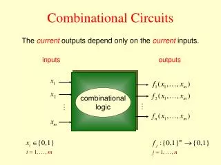
Combinational vs. Sequential Logic Combinational Sequential Output = ( ) f In, Previous In Output = ( ) f In
At every point in time (except during the switching transients) each gate output is connected to either V or V via a low-resistive path. DD ss • The outputs of the gates assumeat all timesthevalue of the Boolean function, implemented by the circuit (ignoring, once again, the transient effects during switching periods). • This is in contrast to the dynamic circuit class, which relies on temporary storage of signal values on the capacitance of high impedance circuit nodes. Static CMOS Circuit
Static Complementary CMOS VDD In1 PMOS only In2 PUN … InN F(In1,In2,…InN) In1 In2 PDN … NMOS only InN PUN and PDN are dual logic networks
NMOS Transistors in Series/Parallel Connection • Transistors can be thought as a switch controlled by its gate signal • NMOS switch closes when switch control input is high
CL CL CL CL Threshold Drops VDD VDD PUN S D VDD D S 0 VDD 0 VDD - VTn VGS PDN VDD 0 VDD |VTp| VGS D S VDD S D
B A C D Complex CMOS Gate OUT = D + A • (B + C) A D B C
Properties of Complementary CMOS Gates Snapshot • High noise margins : V and V are at V and GND , respectively. OH OL DD • No static power consumption : There never exists a direct path between V and DD V ( GND ) in steady-state mode . SS • Comparable rise and fall times: (under appropriate sizing conditions)
CMOS Properties • Full rail-to-rail swing; high noise margins • Logic levels not dependent upon the relative device sizes; ratioless • Always a path to Vdd or Gnd in steady state; low output impedance • Extremely high input resistance; nearly zero steady-state input current • No direct path steady state between power and ground; no static power dissipation • Propagation delay function of load capacitance and resistance of transistors
Rp Rp Rp Rp Rp Rp A A A B B A Cint Rn CL CL CL Rn Rn Rn Rn B A B A A Cint Switch Delay Model Req A A NOR2 INV NAND2
Rp Rp B A Cint CL Rn A Input Pattern Effects on Delay • Delay is dependent on the pattern of inputs • Low to high transition • both inputs go low • delay is 0.69 Rp/2 CL • one input goes low • delay is 0.69 Rp CL • High to low transition • both inputs go high • delay is 0.69 2Rn CL • one input goes high • delay is 0.69 2Rn CL+ Rn Cint or 0.69 2RnCL Rn B
Delay Dependence on Input Patterns A=B=10 A=1 0, B=1 A=1, B=10 Voltage [V] time [ps] NMOS = 0.5m/0.25 m PMOS = 0.75m/0.25 m CL = 100 fF
Rp Rp 2 2 Rp Rp B A B A Rn Cint Cint CL CL Rn Rn Rn B A B A 1 1 Transistor Sizing 4 4 2 2
A D Transistor Sizing a Complex CMOS Gate B 8 6 4 3 C 8 6 4 6 OUT = D + A • (B + C) A 2 D 1 B 2 C 2
D C B A C3 C2 C1 CL Fan-In Considerations A Distributed RC model (Elmore delay) tpHL = 0.69 Reqn(C1+2C2+3C3+4CL) Propagation delay deteriorates rapidly as a function of fan-in – quadratically in the worst case. B C D
quadratic tpHL tp linear tp as a Function of Fan-In Gates with a fan-in greater than 4 should be avoided. tp (psec) tpLH fan-in
tp as a Function of Fan-Out All gates have the same drive current. tpNOR2 tpNAND2 tpINV tp (psec) Slope is a function of “driving strength” eff. fan-out
tp as a Function of Fan-In and Fan-Out • Fan-in: quadratic due to increasing resistance and capacitance • Fan-out: each additional fan-out gate adds two gate capacitances to CL tp = a1FI + a2FI2 + a3FO
C3 C2 C1 CL Fast Complex Gates:Design Technique 1 • Transistor sizing • as long as fan-out capacitance dominates • Progressive sizing Distributed RC line M1 > M2 > M3 > … > MN (the fet closest to the output is the smallest) InN MN In3 M3 In2 M2 Can reduce delay by more than 20%; decreasing gains as technology shrinks In1 M1
C2 C1 C1 C2 CL CL Fast Complex Gates:Design Technique 2 • Transistor ordering critical path critical path 01 charged charged 1 In1 In3 M3 M3 1 1 In2 In2 M2 discharged M2 charged 1 In3 discharged In1 charged M1 M1 01 delay determined by time to discharge CL, C1 and C2 delay determined by time to discharge CL
Fast Complex Gates:Design Technique 3 • Alternative logic structures F = ABCDEFGH
CL CL Fast Complex Gates:Design Technique 4 • Isolating fan-in from fan-out using buffer insertion
Fast Complex Gates:Design Technique 5 • Reducing the voltage swing • linear reduction in delay • also reduces power consumption • But the following gate is much slower! • Or requires use of “sense amplifiers” on the receiving end to restore the signal level (memory design) tpHL= 0.69 (3/4 (CL VDD)/ IDSATn ) = 0.69 (3/4 (CL Vswing)/ IDSATn )
Sizing Logic Paths for Speed • Frequently, input capacitance of a logic path is constrained • Logic also has to drive some capacitance • Example: ALU load in an Intel’s microprocessor is 0.5pF • How do we size the ALU datapath to achieve maximum speed? • We have already solved this for the inverter chain – can we generalize it for any type of logic?
Buffer Example In Out CL 1 2 N (in units of tinv) For given N: Ci+1/Ci = Ci/Ci-1 To find N: Ci+1/Ci ~ 4 How to generalize this to any logic path? Reference: Sutherland, Sproull, Harris, “Logical Effort, Morgan-Kaufmann 1999.
Summary Sutherland, Sproull Harris
Pseudo-NMOS VTC 3.0 2.5 W/L = 4 2.0 p 1.5 [V] W/L = 2 t u p o V 1.0 W/L = 0.5 W/L = 1 p p 0.5 W/L = 0.25 p 0.0 0.0 0.5 1.0 1.5 2.0 2.5 V [V] in
Improved Loads (2) V V DD DD M1 M2 Out Out A A PDN1 PDN2 B B V V SS SS Differential Cascode Voltage Switch Logic (DCVSL)
NMOS-Only Logic 3.0 In Out 2.0 [V] x e g a t l o V 1.0 0.0 0 0.5 1 1.5 2 Time [ns]
NMOS-only Switch V C = 2.5 V C = 2.5 M 2 A = 2.5 V B A = 2.5 V M n B M C 1 L V does not pull up to 2.5V, but 2.5V - V TN B Threshold voltage loss causes static power consumption NMOS has higher threshold than PMOS (body effect)
NMOS Only Logic: Level Restoring Transistor V DD V DD Level Restorer M r B M 2 X M A Out n M 1 • Advantage: Full Swing • Restorer adds capacitance, takes away pull down current at X • Ratio problem
2.0 1.0 0.0 0 100 200 300 400 500 Restorer Sizing 3.0 • Upper limit on restorer size • Pass-transistor pull-downcan have several transistors in stack W / L =1.75/0.25 [V] r e W / L =1.50/0.25 g r a t l o V W / L =1.25/0.25 W / L =1.0/0.25 r r Time [ps]
Solution 2: Single Transistor Pass Gate with VT=0 V DD V DD 0V 2.5V Out 0V V DD 2.5V WATCH OUT FOR LEAKAGE CURRENTS