Download
1 / 4
40 likes | 47 Views
Loop doc for Sen-Sen bonds from Fermilab. Lenny Spiegel Jan 30 th , 2006. FNAL Sen-Sen bonds. FNAL Sen-Sen bonds.

E N D
Loop doc for Sen-Sen bondsfrom Fermilab Lenny Spiegel Jan 30th, 2006
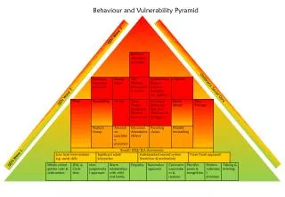
FNAL Sen-Sen bonds • When the issue of sparking arose, in November 2005, we changed our TOB sensor-sensor signal bond profile to increase the height of outer sensor bonds above the n+ implant. At the same time we eliminated 2 out of 6 sensor-sensor bias bonds, which were at the same height as the signal bonds. Thus we have two profiles:1. A "square" profile for the first 76% of TOB modules constructed at FNAL. loop height: 505 microns n+ critical clearance: 140 microns outer sensor (sensor 2)2. A "triange" profile for the last 24% of TOB modules. loop height: 513 microns n+ critical clearance: 286 microns outer sensor
FNAL Sen-Sen bonds • In both cases we are using the first set of bond pads on the sensors (unlike UCSB which switched to second set for their outer sensors when they changed profiles in November 2005). Also, in reporting the above numbers I have subtracted the 25.4 micron diameter of the bonds from the microscope focus measurements as this gives a better indication of the clearance distance. Finally, it should be understood that the above numbers are averages obtained from a limited sample of measurements and that there is a fair amount of variation, so that some n+ clearances are around 100 microns or less.I've enclosed a picture of the "square" profile; don't have one of the "triangle" profile.We are starting a program in the US to encapsulate all sensor-sensor bonds (including the bias bonds) for ALL TOB (and TEC) modules assembled here. In theory the encapsulate material (Dow Corning Sylgard 186) gives a factor of 5-6 improvement on air - for large gaps (~2cm). In practice we find it difficult to show that the encapsulant buys more than a few hundred volts in the maximum operating voltage. However, a few hundred volts is still significant and, in any event, we have started the process.