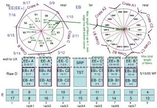
Download
1 / 13
130 likes | 135 Views
EE 365. Introduction, Logic Circuits. Digital Logic. Binary system -- 0 & 1, LOW & HIGH, negated and asserted. Basic building blocks -- AND, OR, NOT. Many representations of digital logic. Transistor-level circuit diagrams Gate symbols (for simple elements). Truth tables Logic diagrams.

E N D
EE 365 Introduction, Logic Circuits
Digital Logic • Binary system -- 0 & 1, LOW & HIGH, negated and asserted. • Basic building blocks -- AND, OR, NOT
Many representations of digital logic • Transistor-levelcircuit diagrams • Gate symbols (for simple elements)
Truth tables • Logic diagrams
Prepackaged building blocks, e.g. multiplexer • Equations: Z = S¢ × A+ S × B
Various hardware description languages ABEL VHDL We’ll start with gates and work our way up
Logic levels • Undefined regionis inherent • digital, not analog • amplification, weak => strong • Switching threshold varies with voltage, temp, process, phase of the moon • need “noise margin” • The more you push the technology, the more “analog” it becomes. • Logic voltage levels decreasing with process • 5 -> 3.3 -> 2.5 -> 1.8 V
MOS Transistors Voltage-controlled resistance PMOS NMOS
CMOS Gate Characteristics • No DC current flow into MOS gate terminal • However gate has capacitance ==> current required for switching (CV2f power) • No current in output structure, except during switching • Both transistors partially on • Power consumption related to frequency • Slow input-signal rise times ==> more power • Symmetric output structure ==> equally strong drive in LOW and HIGH states