Download

1 / 14
140 likes | 279 Views
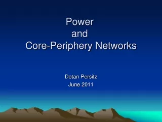
pALPIDEfs Digital periphery. Alberto Collu. University and INFN of Cagliari. Scheme of pALPIDEfs. 1024 columns. Region 0 (16 double columns). Region 1 (16 double columns). Region 30 (16 double columns). Region 31 (16 double columns). 512 rows. ANALOG BIAS. ANALOG BIAS.

E N D
pALPIDEfsDigitalperiphery Alberto Collu University and INFN of Cagliari
SchemeofpALPIDEfs 1024 columns Region 0 (16 double columns) Region 1 (16 double columns) Region 30 (16 double columns) Region 31 (16 double columns) 512 rows ANALOG BIAS ANALOG BIAS RO logic 0 RO logic 1 RO logic 30 RO logic 31 DigitalPeriphery Power, AnalogPads, DigitalPads Alberto Collu
Main operating modes • Configuration mode • Full access to the registers (hamming code, triple voting) and memories • Self Test: automatic test that - identifies double columns where there are faulty pixels - identifies faulty memory locations (containing at least one bit stuck at 0 or 1) • Readout Mode • Matrix readout at trigger arrival • 2 types: Readout mode A , Readout mode B • Features: clustering, on the fly double column disabling • Pattern Generator • Pattern loaded in the data RAMs in config mode • The loaded pattern is sent out throught the data port once Pattern Generator mode starts • Previously thought to be usedto test the serializer, itmay be useful to test the peripherysequentializationlogic (SEU measurements?) Alberto Collu
JTAG Port • Allows read and write access to: • Periphery Registers (for debug and configuration) • Memory locations (no access during readout) • Fully synchronous protocol (10 MHz clock max in pALPIDEfs) • Pads: • TCK : JTAG clock • TMS : JTAG SM control signal • TDI : serial input • TDO : serial output • Possibility to configure chips in a daisy chain • TDI[i] -> TDO[i+1] • TDO[i-1] -> TDI[i] • common TCK and TMS • JTAG operation time duration < 5 us @ 10MHz: • Total time to write all the registers < 1 ms at 10 MHz • Total time to write all the registers/memory locations < 45 ms Alberto Collu
Configuration mode • Bias • 6 voltages , one hot encoding (8 bits) • 5 currents, thermometerencoding (8 bits) • DACMONV and DACMONI pad functionalities • Monitoring • Override (internallygeneratedvoltages and currents can beoverriden) • Matrix readoutdisabling • Regionreadoutdisabling • Doublecolumnreadoutdisabling • In-pixelregisters • Maskregisters • Pulseregisters • State registers • Read and writeof DPRAM memories • 32 DPRAM 16x16 (used in readout mode tostore the lengthofeachevent in eachregion) • 32 DPRAM 256x16 (usedtostore the pixel data in eachevent and in eachregion) Alberto Collu
Readout modes • Readout mode A • In-pixel status registerscontinuouslyenabled • Latch on hit • Readout mode B • In-pixel status registersenabled at trigger arrivalfor a fixedtimeduration • Latch on trigger Alberto Collu
Periphery readout architecture • Columns belonging to a region are read in sequence by the same logic at trigger arrival • Data read in each region is written into a memory • The 32 memories are read sequentially by the same logic 32 regions of 16 double columns each 31 0 15 0 15 0 The readoutofeach reagion isdoneindependently due to the presence of data memories (one per region) Each memory acts as a derandomizing buffer, being written at the trigger arrival and read in a sequence MEM 0 MEM 31 Event Data Port Alberto Collu
Region Readout 32 columns Each region contains 16 double columns A priority encoder in each double column gives a readout order to the hit pixels An end ofcolumnpriority encoder reads in sequence the 16 doublecolumns A clustering algorithm is implemented that reduces the data throughput of the chip The data is written into RAM memories 512 rows Double Column 1 Double Column 0 Double Column 14 Double Column 15 SM Clustering Data memory EvtLenmemory Alberto Collu
Clustering • Notproperly a clusteringbut a data compressionalgorithm • A hit maybeseenas more thanone cluster (forexampleclusterswith hit pixels in 2 adjacentdoublecolumns) • The amountof data per cluster depends on its position and size • Encodes in 16 bits the information of up to 4 consecutive hit pixels • in a doublecolumn: • Pixel address inside of a doublecolumn • Doublecolumnaddress • Cluster size (numberof consecutive hit pixels)
Clustering Seenas 4 separate pixels Seenas 2 clusters of 2 pixelseach Seenas a cluster of 4 pixels Double Column 0 Double Column 14 Double Column 1 Double Column 15 Alberto Collu
Event Data Port • Parallel port • no serializer in this prototype • Dedicated port • output port used to send the event data out of the chip • Pads: • EVT[7:0] : 8-bit wide data bus • EVT VALID : data valid flag • READY : data flow control • Event Data Format (in each region): • Header containing the region number and the event length • Data words containing hit pixel data. The number of data words recorded in an event by a region is given by the event length Alberto Collu
Pulse and Mask operations • Mask operation • Used to mask single pixels in the matrix that are stuck at high value • Normally performed in configuration mode • Not possible to maskautomatically faulty pixels during the readout (entire double columns can be maskedautomatically) • User can mask single pixels, groups of pixels such as rows or columns or the entire matrix even in readout mode if needed - Couldbe useful to keep the priority encoders silent while not reading the matrix (couplinganalog-digital?) • Pulseoperation • Can beusedto test single pixels • Performed in readout mode • Addressingof the pixel tobepulsed via JTAG port • The pulseisprovideddirectlythrough the dedicated PULSE pad • The addressofpulsedpixelsisobtainedbytriggering the chip via the STROBE pad Alberto Collu
Technical difficulties in digital periphery development • Area: • Problemswith low availabilityofhorizonthalroutingchannel • Useof TJ DPRAM memories (height 265 um) routed in 4 metal layers • doesnotallowtohave a verythindigitalperiphery (lessthan 400 um, • 450 um in pALPIDEfs). • Couldbedecreasedbyusing FF basedmemories (50% less • occupancyfor the smallmemories, routingonly in 2 metal layers) Digital periphery height (450 um) TJ memory height (265 um) Alberto Collu
Technical difficulties in digital periphery development • PowerConsumption: • No low powertechniquesadopted (clock gating, disablingofmemories) • Dominatedby: • Switchingof the clock tree • Internalpowerconsumption in the memoryblocks • Estimatedtobe 300 mWfornominalvalues • Couldbedecreasedsignificantly (a factor 5 at least) bydisabling the memorieswhennotused and byadopting a clock gatingscheme (whenpossible) • Timing: • Issues in worstcases due to the widthof the digitalperiphery (3 cm) • Issues in some half-cycle timing paths (memory side) Alberto Collu