Download
1 / 19
190 likes | 400 Views
Cd (Zn)Te X-ray detectors 3D-ASIC project EMFT technology 4040 pixel ASIC Possibility with AIDA WP3. 3D-ASIC development project Paul Seller RAL. 3D-ASIC development. Cd (Zn)Te X-ray pixel detectors. Bump bonding Gold Stud Silver epoxy Imaging applications Dual isotope SPECT

E N D
Cd(Zn)Te X-ray detectors • 3D-ASIC project • EMFT technology • 4040 pixel ASIC • Possibility with AIDA WP3 • 3D-ASIC development project • Paul Seller • RAL
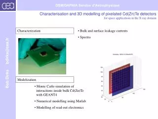
3D-ASIC development Cd(Zn)Te X-ray pixel detectors • Bump bonding • Gold Stud • Silver epoxy • Imaging applications • Dual isotope SPECT • K-edge subtraction • Florescence imaging • Astrophysics • Tumour identification • Illicit materials • TEDDI ASIC gold stud bonded to 3mm CZT and wire bonded to PCB
3D-ASIC development • Cd(Zn)Te detector constraints Some of the charge carriers can be ‘trapped’ in the bulk. This is a ‘noise’ on the signal depending on depth of interaction so use small pixel effect. holes CZT Tailing Q electrons isig One can change bias voltage and thickness but typically electron transit times in CZT can be 100-500ns which gives limits to the shaping time of the signal processing.
+bias X-ray e- h+ P+ diodes 3D-ASIC development • Cd(Zn)Te detector constraints As q drifts in the electric field it also diffuses in all directions. This produces Charge Sharing between pixels and can give rise to ‘tailing’ or multiple hits in photon counting systems. Also the florescence photons can have a similar effect at small pixel sizes. Charge sharing in CZT This either constrains the minimum pixel size or requires detailed charge summing considerations to get good spectral and spatial resolution.
3D-ASIC development Cd(Zn)Te Spectroscopy ASIC • Rolling shutter type readout • Four 80x20 pixel arrays on one ASIC • 250mm x 250mm pixels • Gold stud bonded to CZT • Programmable regions of interest • 12 Analogue outputs • Selectable range 150keV - 1500keV • Noise <1keV FWHM with CZT detector • AMS 0.35um CMOS
3D-ASIC development Cd(Zn)Te Spectroscopy ASIC Pixel Electronics
3D-ASIC development 80 x 80 pixel ASIC and readout card with copper insert With a 50ns clock whole frame readout takes 20x80x50ns =100us/frame =10,000 frames/sec
3D-ASIC development Enclosure with temperature stabilisation and Camera Link output to PC.
3D-ASIC development 80 x 80 pixel spectroscopic ASIC results Pb ring 74keV
3D-ASIC development • If we want more pixels in future:- • analogue tracking problems • more ADCs • slower frame times • If we had ADC per pixel: • no analogue output problem • lots of cross-talk issues • need space in pixel • If we had 3D-ASIC, analogue on top level, digital bottom layer • lots of space • no crosstalk • lots of routing
3D-ASIC development 3D-ASIC project aims:- • To develop the next step in IC signal processing density for HEP, Synchrotrons, Space, medical…… systems • Specifically a 3D-ASIC with two active layers bonded together at many points on surface • Layer 1:- Analogue preamplifiers • Layer 2:- Digital ADCs Progress this year:- • Define a Back-End-of-Line Process with EMFT so we could use different CMOS processes on the different layers. Cu/Sn SLID process with W vias. • Designed and built the 2 layer CMOS wafers for EMFT (IZM Munich) bonding • 40 x 40 pixel detector test ASIC 4040 pixel 3D-ASIC
Extra metal Pad stack Passivation layers Active layer Tungsten TSVs 50um Silicon SLID Cu/Sn/Cu Pad stack Active layer Bottom Silicon 3D-ASIC development Proposed EMFT process
4040 RAL 3D-ASIC Analogue pixel design • Copied from the 8080 pixel readout • 250um pixels • 1keV FWHM with 2us shaping • Dynamic range to 150keV
4040 RAL 3D-ASIC 3D-ASIC Upper pixel Digital pixel design • Lower layer has peak-hold and synchronous 12 bit ADC in every pixel. • Also identifies hit pixels and nearest neighbours • 1600 x 13 bits @ 50MHz = 40 micro second readout 3D-ASIC Lower pixel
4040 RAL 3D-ASIC Upper and lower ASIC on single wafer. (12 wafers made)
4040 RAL 3D-ASIC Upper and lower pixels with via test areas clearly visible
Future plans 2011/2012 Test 2 layers separately with on-chip test circuits Start SLID bonding (2012 finish and test) Require test effort and detailed design of SLID bonding AIDA support for wafers, SLID and collaboration
3D-ASIC development Acknowledgements:- CZT project Matt Wilson Matt Veale (Hexitec funded from EPSRC grant) ASICs Mark Prydderch Peter Murray Matt Hart Lawrence Jones Stephen Thomas Test Alec Hardie
Detector eg. CZT Detector eg. CZT Wire bond Gold studs Gold studs 50um analogueASIC 50um analogueASIC SLID Bonds SLID Bonds Thick digital ASIC Thick digital ASIC Heat sink Heat sink PCB PCB Wire bond Very small dead space 3D-ASIC development • Advanced structure for 4-side butting. • Not yet discussed with EMFT