Download
1 / 37
370 likes | 521 Views
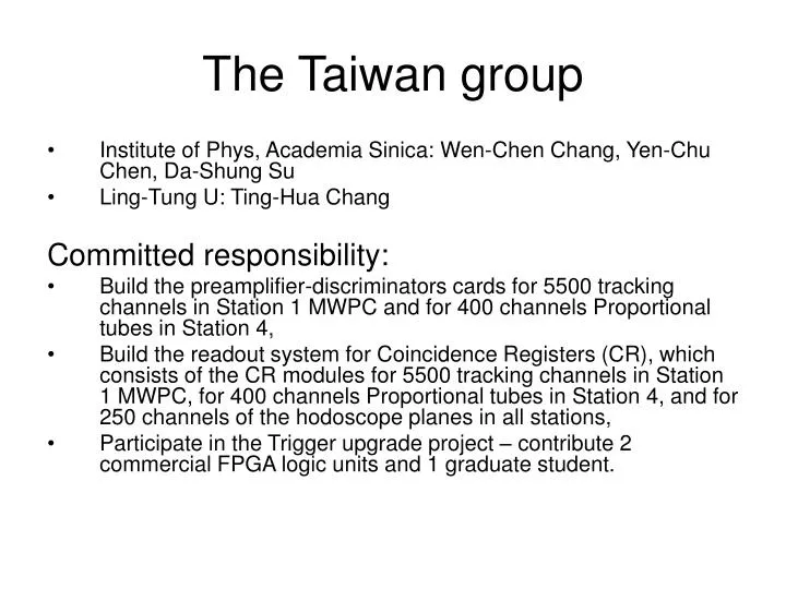
The Taiwan group. Institute of Phys, Academia Sinica: Wen-Chen Chang, Yen-Chu Chen, Da-Shung Su Ling-Tung U: Ting-Hua Chang Committed responsibility: Build the preamplifier-discriminators cards for 5500 tracking channels in Station 1 MWPC and for 400 channels Proportional tubes in Station 4,

E N D
The Taiwan group • Institute of Phys, Academia Sinica: Wen-Chen Chang, Yen-Chu Chen, Da-Shung Su • Ling-Tung U: Ting-Hua Chang Committed responsibility: • Build the preamplifier-discriminators cards for 5500 tracking channels in Station 1 MWPC and for 400 channels Proportional tubes in Station 4, • Build the readout system for Coincidence Registers (CR), which consists of the CR modules for 5500 tracking channels in Station 1 MWPC, for 400 channels Proportional tubes in Station 4, and for 250 channels of the hodoscope planes in all stations, • Participate in the Trigger upgrade project – contribute 2 commercial FPGA logic units and 1 graduate student.
Funding Profile • ~ 300 K USD requested in a 3-year proposal for the hardware from National Science Council of Taiwan • Waiting on approval this July. • Other source: AS Theme Project. 50K USD in addition. Available in the beginning of 2010.
Requirement of PreAmp:Fast, high-gain, low-noise • Initial ionization: 5e (E871 NIM paper) • Gas gain: 10^5 (E871 NIM paper) • 10% of total avalanche charge collected in 10 ns. • 1ns rising time350 MHz BW; 10 ns 35 MHz BW • Input capacitance: 30pF (software simulation of the present layout) • Input impedance:<140 ohm (software simulation of the present layout. From Page 8 at 60MHz) • Charge at circuit input: 5*(1.6*10^-19 C)*(10^5)*0.1=8*10^-15 C=8fC • Current at circuit input: (8*10^-15 C)/10ns= 800 nA • Voltage at circuit input: (8*10^-15 C)/30 pF= 267 V • Trans-impedance gain: 100K ohm (set by chosen components) • Voltage at output: 800nA*100K ohm=80 mV • Gain: 80mV/8fC=10 mV/fC • Voltage Gain: 80mV/267V=300 • Input noise from circuit: < 5.3 V at 35 MHz • < (0.16fC@Cin=30pF)
Input pulse LVDS output Transimpedance amplifier (TIA) Differential amplifier Comparator • Current-Feedback OPA • Low input impedance • High slew rate • Transimpedance gain, Gz=5kΩ • Voltage Gain=20V/V Latch/Hysteresis control Latch input O.C. gate Hysteresis current mirror Currently, the threshold is set by potentiometer on the prototype card. +/-5V DC power supply +5V DC power supply Duplicate to other 15 channels Figure 1. Block diagram of PreAmp-Discriminator Card
Circuit simulation with TINA-TI design software Transimpedance Amplifier Differential Voltage Amplifier Current generator (Current In) Differential voltage out • Input impedance : <140Ω • Transimpedance gain : 100KΩ • -3dB Bandwidth : ~60MHz • Wide linear Input current range : +/-25uA • Differential voltage output swing : +/-2.58V • ESD protection diodes and LVDS comparator are not shown. The simulation result in plots shown in next two pages.
DC analysis AC analysis Small input current vs output voltage Small-signal sine-wave response Large input current vs output voltage Large-signal sine-wave response
AC transfer characteristic Noise analysis Input voltage noise density (without current-limited series resistor, 100Ω) Transimpedance gain vs. frequency Input current noise density (without current-limited series resistor, 100Ω) Input impedance vs. frequency (with current-limited series resistor, 100Ω)
Sensitivity polarity Input signal Positive LVDS output Negative LVDS output Input polarity vs. LVDS output. First use pulse generator as the input Agilent 33120A waveform generator, Tektronix TDS 754D Oscilloscope, +/-5.0V operation for PreAmp card
Input to PreAMP Amplified Signal Comparator Response
Input to PreAMP Amplified Signal Comparator Response
Input to PreAMP Amplified Signal Comparator Response
Input to PreAMP Amplified Signal Comparator Response
Input to PreAMP Amplified Signal Comparator Response
Amplifier / Discriminator Card :IPAS Version • Current-feedback trans-impedance amplifier. • Low input impedance. • Voltage gain = 300. (can be dropped) • RMS of noise level~10mV. • Better reproduce of original input pulse shape. • S/N ratio improved after amplification • Use DAC line to set the threshold is possible and preferred.
Amplifier / Discriminator Card :LANL Version • Voltage-feedback trans-impedance amplifier. • Large input impedance. • Voltage gain = 200. • RMS of noise level~10mV. • Observe long tail of input pulse due to large input impedance.
Input to PreAMP Amplified Signal Comparator Response
Input to PreAMP Amplified Signal Comparator Response
Input to PreAMP Amplified Signal Comparator Response
Questions to be answered • The R-C configuration on the detector side: How to interface between preamp and chamber? • Chamber geometry (pin output arrangement) • Latch frequency: 53MHz? • Voltage gain appropriate? • Threshold of comparator: 0-150 mV (enough?) • Noise level during the run? • Maximum pulse width from MWPC? (signal tail pile up) • Q: Get power from chamber? Separate power supply?
Two possible schemes of preAmp-Latch-CR readout system MWPC—2 preAmp cards—1 Latch-CR VME module—VME Buffered Encoder—VME Event Buffer Interface MWPC—4 preAmp cards—1 Latch-CR Card—VME Event Encoder/Buffer
A Coincidence Register readout system – follow E871 Each detector owns their EB (VME crate?) Parallel paths to EBI for different detectors Design #1
Counting Room Trigger decision • MWPC to electronic platform ~ 100 ft. Exceeds LVDS limit (20m) from preamp • Change preamp output to ECL? ~60ft • Racks on floor OK? Last quad doublet about 200’ upstream
MWPC latch system • Each latch CR module contains: • A total of 32 LVDS inputs • Two 1024x16-bits latch based • shift register • One 2048x32-bits Level-2 • event memory • Read control unit based on • Xilinx Vertex FPGA • NIM signals: Gate, Trigger, Fast clear, Full/Space-available • Standard VME A24/D32 interface • Interrupt • VME 6U backplane Figure 1 Design #1 cont’
Design #1 • Data from PreAmp sent to Latch-CR where the state of each channel is latched with RF clock. • Data are collected to EB then to EBI at L1 trigger with data reduction. If L2 does not occur, clear EBI. • Data in EBI sent out to DAQ at L2 trigger • Delay of digital signals in FPGA and comparator threshold in PreAmp can be remotely adjusted via VME CPU.
# 2 design VME Event Buffer MWPC 5500 channels 16-channel PreAmp/ Discriminator Card 64-channel CR Module Twisted cable Connector DAQ VME crate VME CPU 16-bit LVDS 1 VME Event Buffer Optic fiber 16-bit LVDS 2 Data Compressor 16-bit LVDS driver FPGA Shift Register 16-bit LVDS 3 R/W Lines 16-bit LVDS 4 RF clock Level-1trigger Level 2 Trigger
Design #2 • CR card: • Sits next to PreAmp card and retrieves power from MWPC via LVDS cable connection from PreAmp. • Data clocked into shift registers at RF freq. • With L1 trigger enabled, perform data encoding, and at L2 trigger send data to VME Event Buffer board. • Uses 1 optic fiber for R/W communication with VME Event Buffer board. • Data transfer rate of optic fiber: 1.25Gbps ~ 4.25Gbps • Event Buffer board: • Each EB connects with 16 optic fibers. • Data readout from EB to DAQ at L2 trigger after data is collected from 16 CR cards.
Questions to be answered for #2 • Distance from spectrometer to electronics? • Radiation damage? • L1 & L2 trigger rate? (Is 1 optic fiber enough?)
Information & Estimation • Main Injector RF clock frequency: 53 MHz. • Beam structure: 10^13 protons in a 5 s slow extraction spill every minute. Beam intensity: 2*10^12/sec. • 200 triggers/per spill; 1kHz trigger rate aimed for DAQ. (??) • Level-2 trigger latency: Master Trigger OR decision time= 91ns. • Level-1 trigger rate (X): • MWPC designed Singles rates:53MHz.(?) • The total rate of single muons traversing the detector and passing the trigger matrix tracking will be approximately 100 kHz with the LH2 target and 150 kHz with the LD2 target (both cases include tracks originating in the beam dump). • LVDS clock: minimum 200 MHz. • How many 16-channel preamp cards which one latched module can deal with: (16bit*200MHz)/ (16bit*53MHz)~4. • Event size of MWPC W/O data reduction: 5500bit=0.8kB • Depth of memory buffer: 53MHz*91ns~ 5 events. Size of total memory to buffer 5 events=0.8kB*5=4kB. • VME transfer throughput:0.8kB*1kHz=0.8MB/per sec << Optic fiber ~100 MB/sec and VME 160 MB/sec. Deadtime-free is possible.
Schedule for building PD cards • All R&D and testing work would be done in IPAS electronics lab. • Aug2008 - Jan 2009 – R&D PD card prototype. First few PD prototype cards produced. Test gain, rising time and invest noise pick up. • Jan 2009 – Mar 2009 – Send prototype cards to US collaborator to test with MWPC chamber. Finalize prototype design. • Mar – Aug 2009 – Mass production. Manufacture the rest (~350) cards. Testing. • Aug – Sept 2009 -- All cards shipped to Fermilab for final integration.
Schedule for building CR modules • Aug - Sept 2008 – R&D CR module prototype. First 2 CR prototype modules produced. Develop readout software for multi-boards. • Sept – Dec 2008 – Set up testing environment with a simple DAQ system. Trigger rate will mimic the running condition. Finish testing first set of prototype boards. Finalize prototype design. • Jan – Mar 2009 – Manufacture first 20 boards, test serial/parallel multi-crates readout, test throughputs and event formatting, developing readout software for multi-crates. Set up a DAQ system using JLab CODA in local lab. • Mar – Aug 2009 – Mass production. Manufacture the rest (~ 160) boards. Full system test completed. • Aug – Sept 2009 -- All modules and crates shipped to Fermilab for final integration. • Sept 2009 – Feb 2010 – Crew on site. Install CR modules and PD cards to MWPC. Preparation for the experiment. • Mar 2010 –Scheduled start of E906 data taking? The Ph.D student and Yen-Chu Chen will stay in Fermilab full time.
Conceptual design of DAQ based on CODA MWPC, HODO, Muon Coincidence Register System, VME CAMAC TDC for DC Interface to VME Accelerator scalers, VME? ROC3 ROC2 ROC1 L2 Trigger Electronics House Ethernet Hub Unix host running CODA Counting House Data Decoder Software Data Storage Online monitoring
DAQ • CODA is a DAQ software developed by CEBAF • Provide user interface • Internet based • Event fragment checking & tagging • Flexible configuration, system is easy to expand by adding more ROCs • Reasons to use CODA (open to other options) • Allow all sub-system be developed locally & independently. • Final integration is straightforward. • Technical support available from JLab • Have experienced people among us
DAQ (cont’) • Each sub-system needs a “trigger interface” to synchronize event readout. • Each sub-system needs to develop its readout control code in CODA standard • Need new decoder program. Packet formatter might not be needed. • Need collaborators take responsibilities on each projects. • Final integration and testing of all electronics? (Software + Hardware) Plan and schedule need to be work out.