Download
1 / 9
90 likes | 172 Views
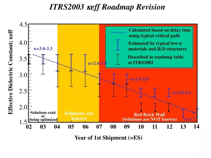
4.5. Calculated based on delay time using typical critical path. 4.0. Estimated by typical low- k materials and ILD structures. k =3.0-3.3. Described in roadmap table at ITRS2002. 3.5. k =2.6-3.0. Effective Dielectric Constant; k eff. 3.0. k =2.4-2.8. 2.5. k =2.0-2.4. 2.0.

E N D
4.5 Calculated based on delay time using typical critical path 4.0 Estimated by typical low-k materials and ILD structures k=3.0-3.3 Described in roadmap table at ITRS2002 3.5 k=2.6-3.0 Effective Dielectric Constant; keff 3.0 k=2.4-2.8 2.5 k=2.0-2.4 2.0 Solutions exist or being optimized Solutions are known Red Brick Wall (Solutions are NOT known) k<1.7 1.5 14 02 03 04 05 06 07 08 09 10 11 12 13 Year of 1st Shipment (=ES) ITRS2003 keff Roadmap Revision
wire wire repeater Critical Path in High-end SoC and RC-scaling Scenario <long IM> <long GM> <short IM> GM with reverse scaled width and thickness wire wire wire wire wire repeater Typical circuits(2NAND+Inv.) connected with average long- intermediate(IM) wires having multiple-stages Global metal(GM) wires with chip-size length divided by optimized repeaters IM wires with module-size length divided by optimized repeaters tmin(1/fmax) µ RTCW+RWCT+2ÖRWCWRTCT Scaling of both RW and CW should be steadily done in order to improve speed (t min) by 30% per generation.
Assumption on Interconnect Parameter Estimation Model <Assumption on Interconnect parameter estimation> Design rule x0.70/node-scaling, Reverse-scaling for GM Chip-size const.(=7mm sq.) as 1-clock cycle limit Module-size x 0.70/node-scaling Repeater Inserted for long IM and GM wires Gate density x 2.0/node(based on ITRS2002 MPU-R.M) Active power density x 0.6/node with average-long IM wire Logic depth x 0.75/node-scaling t min. x 0.70/node-scaling
Impacts of Varying Assumption on Interconnect Parameter < Impact on interconnect parameter > Chip-size RC delay increases, lower keff and r eff are needed Module-size RC delay increases, lower keff and r eff are needed Repeater¯ RC delay drastically increases for long IM and GM wire Total wire length (= number of layers) increases RC delay increases, lower keff and r eff are needed Gate density Power density Lower keff is needed, Jmax/Imax increase Logic depth Lower keff and r eff are needed for IM wire
1 1 1 1 1 1 1 1 1 1 - - - - - 1 7 2 1 6 9 a p a C 1 6 6 l a t o T 1 6 3 1 6 0 B f _ t C a p _ t C a p _ k T r _ I L D _ k V i a _ I L D _ k Sensitivity Analysis of Interconnect Parameters on keff A,C B,C C D Cu Cu Cu D B A: DCL-thickness B: DPL-thickness C: DPL(or DCL)-k D: ILD(Trench)-k E: ILD(Via)-k E A B C E B D A E A B A C Cu D E B D E B C D E M a i n E f f e c t s P l o t ( d a t a m e a n s ) f o r T o t a l C a p a DCL:Dielectric Capping Layer DPL:Dielectric Protection Layer A C D E A C D A B D A B C D C E C D E C D B E B C E • Most sensitive to k of both DPL and DCL • Sensitive to DPL thickness as well as k of ILD (Trench, Via) • Should reduce k and thickness of DPL and DCL as well as k of ILD B C D A D E A D A C E A B E A B C D E A B D E A B C E A B C D E 0 5 1 0
90 nm Node Solutions (2004) Assumptions Cu Cap height = 50nm Hardmask height = NA Via height = 210nm Trench height = 230nm Minimum L/S = 140nm Assumptions Cu Cap height = 50nm Hardmask height = 50nm Via height = 210nm Trench height = 230nm Minimum L/S = 140nm Assumptions Cu Cap height = 50nm Hardmask height = 50nm Via height = 210nm Trench height = 230nm Minimum L/S = 140nm Assumptions k(Cu Cap) = 5.0 k(Hardmask) = NA k(via) = 3.0 k(trench) = 3.0 keff = 3.30 Assumptions k(Cu Cap) = 5.0 k(Hardmask) = 4.1 k(via) = 2.65 k(trench) = 2.65 keff = 3.14 Assumptions k(Cu Cap) = 5.0 k(Hardmask) = 4.1 k(via) = 3.7 k(trench) = 2.65 keff = 3.63
65 nm Node Solutions (2007) Assumptions Cu Cap height = 35nm Hardmask height = NA Via height = 150nm Trench height = 170nm Minimum L/S = 100nm Assumptions Cu Cap height = 35nm Hardmask height = 35nm Via height = 150nm Trench height = 170nm Minimum L/S = 100nm Assumptions Cu Cap height = 35nm Hardmask height = 35nm Via height = 150nm Trench height = 170nm Minimum L/S = 100nm Assumptions k(Cu Cap) = 4.0 k(Hardmask) = NA k(via) = 2.8 k(trench) = 2.8 keff = 2.96 Assumptions k(Cu Cap) = 4.0 k(Hardmask) = 3.0 k(via) = 2.65 k(trench) = 2.65 keff = 2.83 Assumptions k(Cu Cap) = 4.0 k(Hardmask) = 3.0 k(via) = 2.5 k(trench) = 2.4 keff = 2.71
45 nm Node Solutions (2010) Assumptions Cu Cap height = 25nm Hardmask height = NA Via height = 110nm Trench height = 125nm Minimum L/S = 70nm Assumptions Cu Cap height = 25nm Hardmask height = 25nm Via height = 110nm Trench height = 125nm Minimum L/S = 70nm Assumptions Cu Cap height = 25nm Hardmask height = 25nm Via height = 110nm Trench height = 125nm Minimum L/S = 70nm Assumptions k(Cu Cap) = 3.5 k(Hardmask) = NA k(via) = 2.4 k(trench) = 2.4 kkeff = 2.54 Assumptions k(Cu Cap) = 3.5 k(Hardmask) = 2.5 k(via) = 2.2 k(trench) = 2.2 keff = 2.40 Assumptions k(Cu Cap) = 3.5 k(Hardmask) = 2.5 k(via) = 2.2 k(trench) = 2.0 keff = 2.31
Cu Resistivity Increase by Electron-scattering Effect Wire width < mean free path of electrons ¯ Surface scattering dominant p=0 (complete diffuse scattering) p=1 (specular scattering) ¯ Resistivity increases even if Barrier metal is set to zero ¯ BM/Cu interface roughness reduction might be a solution 5 Measured Cu resistivity without BM p=0 4 3 Resistivity(mWcm) p: fraction of electrons having elastic collisions at wire surfaces 2 p=0.5 1 0 0 0.1 0.2 0.3 0.4 0.5 Line width(nm) Red collar legend (Red brick wall) beyond 32nm node (IM pitch=95nm)